I hope you’ve gotten a feel of how we can access the Gameboy Cartridge in Part 1 and now it’s time for the real part that I was looking forward to: Reading the RAM of the cartridge. Before we start I recommend you read Part 1: Reading the ROM.
In this tutorial I’ll still be using my F1RACE game that uses MBC2 which is actually simpler compared to others because some of the other MBC’s use RAM banking; which is just like ROM banking as you should already know if you read Part 1. I’ll also cover another MBC to show how RAM banking works.
When we want to access the SRAM for reading or writing we firstly have to enable the SRAM, this is done by setting RD/WR and sending a specific command to the MBC. The command is called “initialise MBC” which is found on the VBG website and is given to us as 0x0A, this translates to data pins D1 & D3 should be on (00001010). The other thing to take note of is that RD needs to be set to 1 (off) and WR to be set to 0 (on) when we give the 0x0A command.
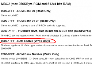
But before we give the “initialise MBC” command we need to know where to write this command to. We hop over to GbdevWiki website and find the address range to enable the RAM: “RAM Enable (Write only)” for MBC2 is 0000-1FFF but they recommend 0000-00FF, so we’ll just use 0000. If you don’t initialise the MBC correctly and then try to read the RAM you will either get the same value when reading all the RAM or get random values both of which I have experienced.
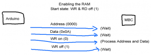
What I have found is that we can actually leave RD and WR as 1 (off), specify the address (0000) and data (0x0A) then turn WR as (0) on and then turn it back off (1). Basically what is happening is we set up the address and data but the MBC doesn’t do anything with it until we turn WR on (0) and that’s when it processes the address and data which makes sense now. This is something to keep in mind because before in Part 1 I wasn’t exactly doing it this way (I was turning on WR/RD before we set up the address/data which worked fine for reading the ROM).
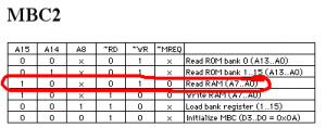
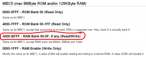
The next step is to find out which address the RAM is at and the values for RD and WR, it looks like it’s at A000-A1FF which would give us 512 values and RD is 0 and WR is 1.
They mention that there are only 4 bits to each value. This is different to how we are used to; normally values would have 8 bits which makes that address value have a byte. So in fact, 512x4bits will really only give us 256bytes of real data. They mention that the 4 bits that data is stored on is the lower 4 bits of the data pins which is D0-D3, so we can ignore the upper 4 bits.
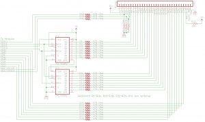
Also we now need to use the CS_RAM or MREQ pin when reading the RAM, it’s the pin after the RD. Our schematic has been updated above to reflex this new pin, same wire up like the WR and RD pins are. When we read the RAM the MREQ pin needs to be 0 (on).
The last step is to disable the RAM, if this isn’t done then you may lose your save data if you disconnect the cartridge from the power. Looking at the addresses website, we disable the RAM by writing 0x00 to the same address we enabled the RAM at: 0000. After this we are free to remove the cartridge or turn the power off.
Read MBC2 RAM
Now for the code.
int latchPin = 10;
int dataPin = 11;
int clockPin = 12;
int rdPin = A5;
int wrPin = 13;
int mreqPin = A4;

void setup() {
  Serial.begin(57600);
  pinMode(latchPin, OUTPUT);
  pinMode(clockPin, OUTPUT);
  pinMode(dataPin, OUTPUT);
  pinMode(rdPin, OUTPUT);
  pinMode(wrPin, OUTPUT);
  pinMode(mreqPin, OUTPUT);
  for (int l = 2; l <= 9; l++) {
    pinMode(l, INPUT);
  }
}
Just the assignment of pins and our standard setup like last time. Note that our new MREQ pin is assigned to Analog Pin 4 on the Arduino. a new we just have a for loop this time for the input pins.
void loop() {

  // Wait for serial input
  while (Serial.available() <= 0) {
    delay(200);
  }
  Serial.flush();
On to the loop, I have added a wait until the Arduino receives some serial input before it starts so this lets us change cartridges without needing to power off or reset the Arduino. The serial input will come from our Python script.
  // MBC2 Fix (unknown why this fixes it, maybe has to read ROM before RAM?)
  digitalWrite(wrPin, HIGH); // WR off
  digitalWrite(latchPin, LOW);
  shiftOut(dataPin, clockPin, MSBFIRST, (0x0134 >> 8));
  shiftOut(dataPin, clockPin, MSBFIRST, (0x0134 & 0xFF));
  digitalWrite(latchPin, HIGH);
Now this next part is something that I spent a few days trying to figure out, after a lot of testing I came up with the above code. For some unknown reason if you don’t perform the above and you have a MBC2 cartridge then it won’t read the first few values correctly. Maybe MBC requires you to read the ROM before the RAM, who knows. A MBC5 cartridge works fine without it.
  Serial.println("START");

  // Turn everything off
  digitalWrite(rdPin, HIGH); // RD off
  digitalWrite(wrPin, HIGH); // WR off
  digitalWrite(mreqPin, HIGH); // MREQ off
We have START command so our Python script knows when to start saving data as the RAM. As per our new findings, we turn everything off before we start doing anything.
unsigned int addr = 0; // Now we really need to use unsigned
Remember how in the last part I said we would be better off using an unsigned int even though a “normal” int would work? Now we really need an unsigned int because RAM reading starts at 0xA000 which is 40,960 in decimal and if we used the “normal” int it would overflow to -24,576.
  // Shift out 0x0000
  digitalWrite(latchPin, LOW);
  shiftOut(dataPin, clockPin, MSBFIRST, (addr >> 8));
  shiftOut(dataPin, clockPin, MSBFIRST, (addr & 0xFF));
  digitalWrite(latchPin, HIGH);
  delay(1);

  // Set D0-D7 pins as outputs
  for (int l = 2; l <= 9; l++) {
    pinMode(l, OUTPUT);
  }
Using our shift registers we shift out 0x0000 and set out data pins to outputs.
  // Initialise MBC: 0x0A
  digitalWrite(3, HIGH);
  digitalWrite(5, HIGH);
  digitalWrite(wrPin, LOW); // WR on
  digitalWrite(wrPin, HIGH); // WR off
Now we initialise the MBC so we can read the RAM, by turning on pins 3 and 5 on the Arduino we are really turning on D1 and D3 on the gameboy cartridge and that gives us 0x0A (00001010). WR is set to low (on) so the MBC processes our request and we set it back to high (off)
  // Turn outputs off and change back to inputs
  for (int l = 2; l <= 9; l++) {
    digitalWrite(l, LOW);
    pinMode(l, INPUT);
  }
We just turn off the outputs and set the data pins back to inputs.
  // Read RAM (512 addresses)
  for (addr = 0xA000; addr <= 0xA1FF; addr++) {
    digitalWrite(latchPin, LOW);
    shiftOut(dataPin, clockPin, MSBFIRST, (addr >> 8));
    shiftOut(dataPin, clockPin, MSBFIRST, (addr & 0xFF));
    digitalWrite(latchPin, HIGH);
    delayMicroseconds(50);
This part should look similar to how we read the ROM, we have changed the for loop to start at 0xA000 and end at 0xA1FF for the 512 values in MBC2. Another way to say it would be 512 nibbles as the MBC2 RAM only is stored on 4 bits – a nibble is half a byte.
    // Tell MBC to process our RAM request
    digitalWrite(mreqPin, LOW); //MREQ on
    digitalWrite(rdPin, LOW); // RD on
By setting MREQ and RD pins to low (on) we are telling the MBC to process our RAM request.
    byte bval = 0xF0; // Upper 4 bits always high (11110000)
    for (int z = 5; z >= 2; z--) { // Read only 4 lower bits
      if (digitalRead(z) == HIGH) {
        bitWrite(bval, (z-2), HIGH);
      }
    }
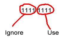
Now we can read the data pins. We remember that there are 4 bits (not 8 ) to each of those values and that the data is in the lower 4 bits, so we need to change our reading code. Firstly set the upper 4 bits to high by assigning bval as 0xF0 which would give us 1111 0000 meaning that the lower 4 bits are unchanged. Next we only read data pins D0-D3 by changing our start value to 5 in the for loop.
    // Done reading this part of RAM
    digitalWrite(mreqPin, HIGH); //MREQ off
    digitalWrite(rdPin, HIGH); // RD off

    Serial.println(bval, DEC);
  }
  Serial.println("END");
After we have read the data pins, we set MREQ and RD back to high (off) and the rest is the same as before, we print the value as a decimal and print END to tell our Python script to stop.
  // Disable RAM
  addr = 0;
  digitalWrite(latchPin, LOW);
  shiftOut(dataPin, clockPin, MSBFIRST, (addr >> 8));
  shiftOut(dataPin, clockPin, MSBFIRST, (addr & 0xFF));
  digitalWrite(latchPin, HIGH);
  delay(1);

  // Set D0-D7 pins as outputs
  for (int l = 2; l <= 9; l++) {
    pinMode(l, OUTPUT);
    digitalWrite(l, LOW);
  }
It’s time to disable the RAM, as before we will be writing to the address 0x0000 and we our data pins to outputs and set them all to 0 as we will be writing 0x00.
  // Tell MBC to process our request
  digitalWrite(wrPin, LOW); // WR 0
  digitalWrite(wrPin, HIGH); // WR 1

  // Set pins back to inputs
  for (int l = 2; l <= 9; l++) {
    pinMode(l, INPUT);
  }
}
We now set WR to low (on) and then high (off) for the MBC to process our request and then set the data pins back to inputs.
Test the F1RACE save game
Firstly download iG_GBCartRead_Read_RAM_Only and then upload the iG_GBCartRead_Read_RAM_Only_Arduino.pde file to the Arduino and run the iG_GBCartRead_Read_RAM_Only_Script.py Python script either by double clicking it or editing and pressing F5.
It should only take a few seconds and we’ll have a file called mbc2save.sav created.
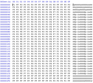
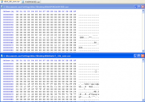
We’ll open that up with our hex editor, looks like there is data in there.
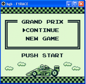
Now we can actually test that we have the complete F1RACE save game by loading our F1RACE ROM into the emulator, you did dump your ROM right? :). Copy mbc2save.sav to F1RACE.sav and then load up BGB (a gameboy emulator) and BGB should find the save file.
Yes, it works!
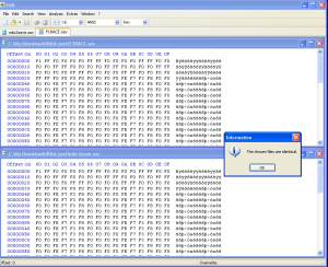
Another way to check is to delete F1RACE.sav, then load F1RACE in BGB again except this time it will make it’s own save game. Now we can compare our mb2save.sav with it. Note that this might not work all the time because some emulators don’t make the exact same file as the Gameboy but you will see some similarities. For F1RACE it does and they are exactly the same.
Read MBC5 RAM using RAM banking
Now we’ll modify our code to use RAM banking on a MBC5 cartridge which has 32Kbytes – my cartridge of choice is Pokemon Red because it contains data outside the first 8Kbytes when you start a new game so you can easily verify your save with the emulators save.
The RAM is grouped in 8K blocks with 4 banks. The GbdevWiki website says that the start address for MBC5 is still A000 but the end address changes to BFFF to fit the 8Kbytes (BFFF – A000 = 8,191 + 1 for starting at A000). Once we have read the first 8Kbytes block of RAM just fine but we need to be able to switch to the next 8K and so on. We do this by writing to the address 0x4000 and using the data pins to specify the bank to read which should sound familiar to you.
...

  // Initialise MBC: 0x0A
  digitalWrite(3, HIGH);
  digitalWrite(5, HIGH);
  digitalWrite(wrPin, LOW); // WR on
  digitalWrite(wrPin, HIGH); // WR off

  // Turn outputs off and change back to inputs
  for (int l = 2; l <= 9; l++) {
    digitalWrite(l, LOW);
    pinMode(l, INPUT);
  }

  // Switch banks (32Kbytes)
for (int bank = 0; bank <= 3; bank++) {

// Shift out 0x4000
digitalWrite(latchPin, LOW);
shiftOut(dataPin, clockPin, MSBFIRST, (0x4000 >> 8));
shiftOut(dataPin, clockPin, MSBFIRST, (0x4000 & 0xFF));
digitalWrite(latchPin, HIGH);
delayMicroseconds(50);

// Set D0-D7 pins as outputs
for (int l = 2; l <= 9; l++) {
pinMode(l, OUTPUT);
}

if (bank & 1) {
digitalWrite(2, HIGH);
}
if (bank & 2) {
digitalWrite(3, HIGH);
}

// Tell MBC to process our RAM bank request
digitalWrite(wrPin, LOW); // WR 0
digitalWrite(wrPin, HIGH); // WR 1

// Turn outputs off and change back to inputs
for (int l = 2; l <= 9; l++) {
digitalWrite(l, LOW);
pinMode(l, INPUT);
}

    // Read RAM
    for (addr = 0xA000; addr <= 0xBFFF; addr++) {
      digitalWrite(latchPin, LOW);
      shiftOut(dataPin, clockPin, MSBFIRST, (addr >> 8));
      shiftOut(dataPin, clockPin, MSBFIRST, (addr & 0xFF));
      digitalWrite(latchPin, HIGH);
      delayMicroseconds(50);

...
There isn’t too much of a code change as all that’s needed is a for loop to happen 4 times. We shift out to the 0x4000 address, set our data pins as outputs and by using the AND (&) we can determine which data pins to turn on. We enable (0) and then disable (1) the WR pin so the MBC can process our request then set our data pins back to inputs. The only other thing that changes is to set our end address in the reading RAM loop is set to BFFF and that’s it.
Download iG_GBCartRead_Read_32K_RAM_Only1 and then upload the iG_GBCartRead_Read_32K_RAM_Only_Arduino.pde file to the Arduino and run the iG_GBCartRead_Read_32K_RAM_Only_Script.py Python script. After a few seconds and we’ll have a file called mbc5_32k_save.sav created.
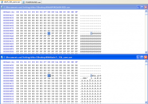
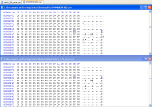
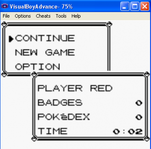
Now let’s compare this file with the VBA emulator version which is at the same state as the Gameboy (I chose the VBA emulator because BGB appears to write random data when it could be just padded with FF to make it easier to distinguish real data from null data). It might not all match but there are specific sections that do so we know we have a good save.
Last test load it up in the emulator and yes it also works too!
And that’s it, now we are able to read the RAM of our cartridges. In my next part I’ll show you how we can write to the RAM so then we can restore our game saves, it’s pretty simple actually and we can use the same code for reading just swap values of RD and WR then set the data pins to outputs but that’s for next time.
GBCartRead Part 1: Read the ROM
GBCartRead Part 2: Read the RAM
GBCartRead Part 3: Write to RAM
GBCartRead: Completed
Gameboy Cart Shield released
Buy the Gameboy Cart Shield
Emulating the Nintendo Logo on the Gameboy
In this tutorial I’ll still be using my F1RACE game that uses MBC2 which is actually simpler compared to others because some of the other MBC’s use RAM banking; which is just like ROM banking as you should already know if you read Part 1. I’ll also cover another MBC to show how RAM banking works. Before we start I recommend you read Part 1: Reading the ROM.
When we want to access the SRAM for reading or writing we firstly have to enable the SRAM, this is done by setting RD/WR and sending a specific command to the MBC. The command is called “initialise MBC” which is found on the GB cart website and is given to us as 0x0A, this translates to data pins D1 & D3 should be on (00001010). The other thing to take note of is that RD needs to be set to 1 (off) and WR to be set to 0 (on) when we give the 0x0A command.
But before we give the “initialise MBC” command we need to know where to write this command to. We hop over to the other useful website with address ranges and find the address range to enable the RAM: “RAM Enable (Write only)” for MBC2 is 0000-1FFF but they recommend 0000-00FF, so we’ll just use 0000. If you don’t initialise the MBC correctly and then try to read the RAM you will either get the same value when reading all the RAM or get random values both of which I have experienced.
What I have found is that we can actually leave RD and WR as 1 (off), specify the address (0000) and data (0x0A) then turn WR as (0) on and then turn it back off (1). Basically what is happening is we set up the address and data but the MBC doesn’t do anything with it until we turn WR on (0) and that’s when it processes the address and data which makes sense now. This is something to keep in mind because before in Part 1 I wasn’t exactly doing it this way.
The next step is to find out which address the RAM is at, it looks like it’s at A000-A1FF which would give us 512 values however they mention that there are only 4 bits to each value. This is different to how we are used to; normally values would have 8 bits which makes that address value have a byte. So in fact, 512x4bits will really only give us 256bytes of real data. They mention that the 4 bits that data is stored on is the lower 4 bits of the data pins which is D0-D3, so we can ignore the upper 4 bits.
Also we now need to use the CS_RAM or MREQ pin when reading the RAM, it’s the pin after the RD. Our schematic has been updated as below to reflex this new pin, same wire up like the WR and RD pins are. When we read the RAM the MREQ pin needs to be low (0).
The last step is to disable the RAM, if this isn’t done then you may lose your save data if you disconnect the cartridge from the power. Looking at the addresses website, we disable the RAM by writing 0x00 to the same address we enabled the RAM at: 0000. After this we are free to remove the cartridge or turn the power off.
Read MBC2 RAM
Now for the code.
int latchPin = 10;

int dataPin = 11;

int clockPin = 12;

int rdPin = A5;

int wrPin = 13;

int mreqPin = A4;

void setup() {

  Serial.begin(57600);

  pinMode(latchPin, OUTPUT);

  pinMode(clockPin, OUTPUT);

  pinMode(dataPin, OUTPUT);

  pinMode(rdPin, OUTPUT);

  pinMode(wrPin, OUTPUT);

  pinMode(mreqPin, OUTPUT);

  for (int l = 2; l <= 9; l++)
{

    pinMode(l, INPUT);

  }

}
Just the assignment of pins and our standard setup like last time. Note that our new MREQ pin is assigned to Analog Pin 4 on the Arduino. a new we just have a for loop this time for the input pins.
void loop() {


  // Wait for serial input

  while (Serial.available() <=
0) {

    delay(200);

  }

  Serial.flush();
On to the loop, I have added a wait until the Arduino receives some serial input before it starts so this lets us change cartridges without needing to power off or reset the Arduino. The serial input will come from our Python script.
  // MBC2 Fix (unknown why
this fixes it, maybe has to read ROM before RAM?)

  digitalWrite(wrPin, HIGH); //
WR 1

  digitalWrite(latchPin, LOW);

  shiftOut(dataPin, clockPin,
MSBFIRST, (0x0134 >> 8));

  shiftOut(dataPin, clockPin,
MSBFIRST, (0x0134 & 0xFF));

  digitalWrite(latchPin, HIGH);
Now this next part is something that I spent a few days trying to figure out, after a lot of testing I came up with the above code. For some unknown reason if you don’t perform the above and you have a MBC2 cartridge then it won’t read the first few values correctly. Maybe MBC requires you to read the ROM before the RAM, who knows. A MBC5 cartridge works fine without it.
Serial.println("START");

  // Turn everything off

  digitalWrite(rdPin, HIGH); //
RD off

  digitalWrite(wrPin, HIGH); //
WR off

  digitalWrite(mreqPin, HIGH); //
MREQ off
We have START command so our Python script knows when to start saving data as the RAM. As per our new findings, we turn everything off before we start doing anything.
  unsigned int addr = 0; //
Now we really need to use unsigned
Remember how in the last part I said we would be better off using an unsigned int even though a “normal” int would work? Now we really need an unsigned int because RAM reading starts at 0xA000 which is 40,960 in decimal and if we used the “normal” int it would overflow to -24,576.
  // Shift out 0x0000

  digitalWrite(latchPin, LOW);

  shiftOut(dataPin, clockPin,
MSBFIRST, (addr >> 8));

  shiftOut(dataPin, clockPin,
MSBFIRST, (addr & 0xFF));

  digitalWrite(latchPin, HIGH);

  delay(1);


  // Set D0-D7 pins as outputs

  for (int l = 2; l <= 9; l++)
{

    pinMode(l, OUTPUT);

  }
Using our shift registers we shift out 0x0000 and set out data pins to outputs.
  // Initialise MBC: 0x0A

  digitalWrite(3, HIGH);

  digitalWrite(5, HIGH);

  digitalWrite(wrPin, LOW); // WR
on

  digitalWrite(wrPin, HIGH); //
WR off
Now we initialise the MBC so we can read the RAM, by turning on pins 3 and 5 on the Arduino we are really turning on D1 and D3 on the gameboy cartridge and that gives us 0x0A (00001010). WR is set to low (on) so the MBC processes our request and we set it back to high (off)
  // Turn outputs off and
change back to inputs

  for (int l = 2; l <= 9; l++)
{

    digitalWrite(l, LOW);

    pinMode(l, INPUT);

  }
We just turn off the outputs and set the data pins back to inputs.
  // Read RAM (512
addresses)

  for (addr = 0xA000; addr <=
0xA1FF; addr++) {

    digitalWrite(latchPin, LOW);

    shiftOut(dataPin, clockPin,
MSBFIRST, (addr >> 8));

    shiftOut(dataPin, clockPin,
MSBFIRST, (addr & 0xFF));

    digitalWrite(latchPin, HIGH);

    delayMicroseconds(50);
This part should look similar to how we read the ROM, we have changed the for loop to start at 0xA000 and end at 0xA1FF for the 512 values in MBC2. Another way to say it would be 512 nibbles as the MBC2 RAM only is stored on 4 bits – a nibble is half a byte.
    // Tell MBC to process
our RAM request

    digitalWrite(mreqPin, LOW);
//MREQ on

    digitalWrite(rdPin, LOW); //
RD on
By setting MREQ and RD pins to low (on) we are telling the MBC to process our RAM request.
    byte bval = 0xF0; //
Upper 4 bits always high (11110000)

    for (int z = 5; z >= 2;
z--) { // Read only 4 lower bits

      if (digitalRead(z) == HIGH)
{

        bitWrite(bval, (z-2),
HIGH);

      }

    }
Now we can read the data pins. We remember that there are 4 bits (not 8) to each of those values and that the data is in the lower 4 bits, so we need to change our reading code. Firstly set the upper 4 bits to high by assigning bval as 0xF0 which would give us 1111 0000 meaning that the lower 4 bits are unchanged. Next we only read data pins D0-D3 by changing our start value to 5 in the for loop.
    // Done reading this
part of RAM

    digitalWrite(mreqPin, HIGH);
//MREQ off

    digitalWrite(rdPin, HIGH); //
RD off


    Serial.println(bval, DEC);

  }


Serial.println("END");
After we have read the data pins, we set MREQ and RD back to high (off) and the rest is the same as before, we print the value as a decimal and print END to tell our Python script to stop.
  // Disable RAM

  addr = 0;

  digitalWrite(latchPin, LOW);

  shiftOut(dataPin, clockPin,
MSBFIRST, (addr >> 8));

  shiftOut(dataPin, clockPin,
MSBFIRST, (addr & 0xFF));

  digitalWrite(latchPin, HIGH);

  delay(1);


  // Set D0-D7 pins as outputs

  for (int l = 2; l <= 9; l++)
{

    pinMode(l, OUTPUT);

    digitalWrite(l, LOW);

  }
It’s time to disable the RAM, as before we will be writing to the address 0x0000 and we our data pins to outputs and set them all to 0 as we will be writing 0x00.
  // Tell MBC to process
our request

  digitalWrite(wrPin, LOW); // WR
0

  digitalWrite(wrPin, HIGH); //
WR 1


  // Set pins back to inputs

  for (int l = 2; l <= 9; l++)
{

    pinMode(l, INPUT);

  }

}
We now set WR to low (on) and then high (off) for the MBC to process our request and then set the data pins back to inputs.
Test our F1RACE save game
Firstly we upload the iG_GBCartRead_RAM_Only.pde file to the Arduino and then run the iG_GBCartRead_RAM_Only.py Python script.
It should only take a few seconds and we’ll have a file called mbc2save.sav created.
We’ll open that up with our hex editior, looks like there is data in there.
Now we can actually test that we have the complete F1RACE save game by loading our F1RACE ROM into the emulator, you did dump your ROM right? :). Change mbc2save.sav to F1RACE.sav and then load up BGB (a gameboy emulator) and BGB should find the save file.
Yes, it works!
Read MBC5 RAM using RAM banking
Now we’ll modify our code to use RAM banking on a MBC5 cartridge which has 32Kbytes – my cartridge of choice is Wario Land 3. There is only a slight code change that needs to be done.


[…] part won’t be as large as our previous parts because we’re really just re-using our Reading the RAM code. Let’s jump right to the […]