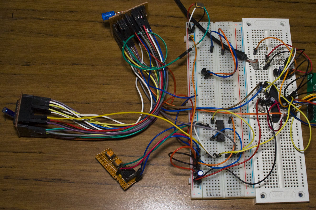
From our last part we switched tested the Cypress 1Mbit SRAM and read the data out with an Olimex STM32 board. In this part we’ll move to an ATmega to read out the data and use it for triggering the CPLD which will be continually sampling the inputs – the reason is because the ATmega runs slower than the CPLD so a few clock cycles will occur from when it detects the trigger to when it signals the CPLD.
CPLD Side
On the CPLD we can remove the data pins which were being used to test the SRAM and we can link WE and OE pins directly to the SRAM. We’ll re-use the writing pin to tell the CPLD to start capturing data or to be in the read mode, another pin for when we want it to trigger and it records the address minus 50 so that we can see some data before the trigger event.
always @ (posedge clockin) begin
	// Reset condition
	...
	// Start writing and wait for a trigger as long as the capture isn't finished
		if (writing && !capturedone) begin
			we <= 1'b0;
			oe <= 1'b1;
			readinginit <= 1'b1;
			address <= address + 17'b1;

			// Triggered, save the starting address
			if (startcapture && startcaptureinit) begin
				startaddress <= address - 17'd50;
				startcaptureinit <= 1'b0;
			end

			// Current address is now the start address, stop the capture
			if (startcapture && (startaddress == address)) begin
			  capturedone <= 1'b1;
			end
		end

		// Start reading
		else if (!writing) begin
			oe <= 1'b0;
			we <= 1'b1;

			// Initialise the starting read address as the start of the capture
			if (readinginit == 1) begin
				readinginit <= 1'b0;
				address <= startaddress;
			end

			// Increment address by 1 when we receive a low and then high clock
			else if (nextaddress == 1 && nextaddresswait == 0) begin
				nextaddresswait <= 1'b1;
				address <= address + 17'b1;
			end
			else if (nextaddress == 0) begin
				nextaddresswait <= 1'b0;
			end
		end
	end
end
As you can see if we are in the writing part and the capture isn’t complete, we increment the address and are constantly writing to the SRAM. When we trigger start capture on the MCU side, we write the address minus 50 to the start address so we can see some sampling before the trigger occurred and once we reach the start address then we stop the writing. When we aren’t writing, we’re reading so we initialise the address to be the start address and increment the address when the MCU wants – the MCU will be responsible for keeping track of the addresses.
When compiling this in Quartus I kept receiving a warning saying “Macrocell buffer inserted after node”
(ID: 163076). If you moved the item it warned you about to a different pin it would warn you about another pin.
![]()
Eventually I found in the assignment editor that instead of picking a location yourself, you can let Quartus pick the best pin based on the optimisation of speed and it worked fine. However when you add extra registers or input/output pins it can affect which pins it chooses for the optimisation, it can just change them all so you need to be careful as if you have your PCB already this would make you have to start over.
I was lucky and managed to switch back to location based pins for my address pins after added the “capture done” routine and it didn’t give me a warning this time, it should make it easier to route on the PCB.
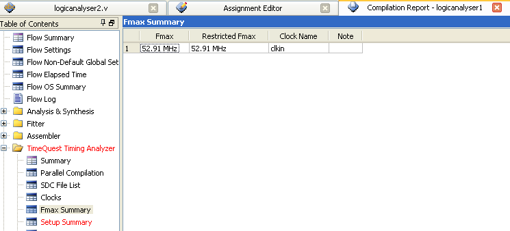
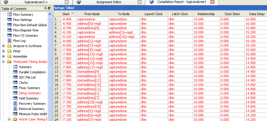
The maximum frequency that’s reported by the timing analyser shows as 52MHz though when checking out the slack times, the most limiting factor is the capturedone to address with a data delay of 14 to 16ns so that shouldn’t be too much of a concern because it’s really just used to tell us when the capturing is complete but address to address delays are 11.3 ns which could be an issue at 100MHz.
Download logicanalyser1
.
ATmega Side
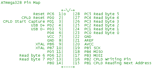
For the ATmega side we will be using V-USB, the 8 inputs to the SRAM will also go to our ATmega so that it can read back the data and later on trigger based on signals we receive. We’ve got out CPLD reset, start capture, writing and next address pins which connect to the CPLD. I’m running the ATmega at the quickest it can – 20MHz so we can read the SRAM as fast. The writing pin also connects to a 74HC125 buffer which lets a clock through to the SRAM when writing and disables it when writing has finished.
_delay_ms(500);  // Wait for CPLD clock to stablise

PORTB |= (1<<writingPin); // Tell CPLD to start capturing data
PORTD |= (1<<cpldresetPin);
_delay_us(10); // Simulate waiting for a trigger

PORTD |= (1<<startcapturePin); // Trigger the CPLD to write the start address of our capture
_delay_ms(5); // Wait 5ms for the capture

PORTB &= ~(1<<writingPin); // Finish writing
PORTD &= ~(1<<startcapturePin);
_delay_ms(5);

startUSB(); // Transfer data
transferData();
usbDeviceDisconnect();
Here we just do exactly what we discussed the CPLD will do for us, after we trigger the CPLD we wait for 5ms to finish it going through all the addresses.
#define USB_TRANSFER 1
static uchar replyBuf[254];
...

// Loop 125 (x2 bytes) times to send this data over USB
for (int a = 0; a < 125; a++) {
	PORTB |= (1<<nextaddressPin); // Tell the CPLD we want the next address

	// Read PD7-6 & PC6-0 and convert the two 4 bytes to hex
	uint8_t lowbyteReading = (PINC & 0x0F);
	uint8_t highbyteReading = ((PIND & 0xC0) | (PINC & 0x30)) >> 4;
	if (lowbyteReading < 10) {
		lowbyteReading = lowbyteReading + 48;
	}
	else {
		lowbyteReading = 'A' + lowbyteReading - 10;
	}
	if (highbyteReading < 10) {
		highbyteReading = highbyteReading + 48;
	}
	else {
		highbyteReading = 'A' + highbyteReading - 10;
	}
	*++nextDigit = highbyteReading; // Add both bytes to reply buffer
	*++nextDigit = lowbyteReading;

	PORTB &= ~(1<<nextaddressPin);

	// Count until the end of the SRAM
	if (counting >= endCount) {
		inusbTransfer = false;
	}
	counting++;
}
*++nextDigit = '\0';

usbMsgPtr = replyBuf;
return sizeof(replyBuf);
I have used V-USB before for my other projects but I’ve only been sending 1 piece of data at a time which only happens once every 15ms (USB 1.1) which is pretty slow. We can simply increase our buffer and fit more data in each transfer it does – from 1-3 bytes to 250 bytes.
Instead of sending our 8 bits of data like 10101101 which would take up 1 byte per bit when transferring it over, I opted for splitting the bits into 2x 4bits and converting each 4 bits to hex, now all we do is send the hex value which would just take 2 bytes, the above would give us 0xAD.
When programming the ATmega at the moment I need to disconnect everything from the CPLD/SRAM as it’s only 3.3V logic, so I’ll have to add a logic level converter as I’m very likely going with an SMD ATmega.
Download CPLD_Logic_Analyser_v0.2
.
Testing
------------- 0 times, 1.#INF00 mhz
------------------------ low
------------- 82 times, 0.609756 mhz
------------- 108 times, 0.462963 mhz
------------- 107 times, 0.467290 mhz
------------- 2 times, 25.000000 mhz
------------------------ low
------------- 0 times, 1.#INF00 mhz
------------------------ low
------------- 115 times, 0.434783 mhz
------------- 111 times, 0.450450 mhz
------------- 114 times, 0.438596 mhz
------------- 109 times, 0.458716 mhz
------------- 109 times, 0.458716 mhz
------------- 112 times, 0.446429 mhz
------------- 109 times, 0.458716 mhz
------------- 92 times, 0.543478 mhz
------------- 111 times, 0.450450 mhz
After extracting the data from the SRAM, the file is just a bunch of 1 and 0’s (00 means low, 01 means high) as I’m just sampling 1 pin on the SRAM. I wrote a little program to count the 1’s and 0’s in a row and we can calculate frequency by dividing 1,000 by the result. For example, the above would mean that we have a high of 0.43 MHz and low of 0.45MHz which gives us a clock of 220KHz, close to the 250KHz my clock is running at. One problem is that I seem to be getting quite a bit of noise (the “0” times or 92 times). Download logic_analyser_extract and parse_logic.
When re-reading a section of the SRAM over and over again, it doesn’t always give the same results and checking with an oscilloscope does confirm this, I may have a layout a board to join up the CPLD, SRAM and oscillator. Most likely it will be a plug in board so I can swap any part as needed and don’t have to re-solder the CPLD/SRAM to the board itself as they would be on sub-boards.
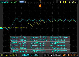
Also there is a visible delay from when the ATmega sends the next address high signal (blue) to when the SRAM gives us the correct result. It’s 40ns for the data result to begin being correct and a total of 80-100ns for it to stablise. I’m hoping this can improve when laying out a new PCB.
I also tried a 100MHz oscillator instead of the 50MHz I was using and it seems that the data I read back was random. After reading the Cypress SRAM datasheet, it appears that you have to hold the CS line low for a minimum of 8ns. At 50MHz, the clock low is 10ns (clock high 10ns) so that works but then at 100MHz, clock low is now 5ns which is why I believe it didn’t work.
Another feature which I’m thinking of adding is having the ATmega with a timer to generate a clock signal lower than 10MHz which will be feed into the CPLD as the main clock when required and we would switch off the main 50MHz oscillator. This means that instead of taking just 2.6ms to sample the 8 channels at 50MHz we can switch to a lower clock and have it sample for more time.
That’s all for the moment until I make a new PCB, add in the extra buffer and make the clock to the CPLD selectable.
Building a CPLD Based Logic Analyser – Part 1: SPI writing in Verilog, Testing the basics and modifying Scanalogic SCL files to insert our own data
Building a CPLD Based Logic Analyser – Part 2: Switching to the EPM3064 CPLD
Building a CPLD Based Logic Analyser – Part 3: Testing the Cypress 1Mbit SRAM
Building a CPLD Based Logic Analyser – Part 4: Reading data/triggering with an ATmega with V-USB and testing
Building a CPLD Based Logic Analyser – Part 5: Prototype boards and fixing reading issues
Building a CPLD Based Logic Analyser – Part 6: Software side, trigger/sampling options, hardware changes and possible changes for a 100MHz analyser
Building a CPLD Based Logic Analyser – Part 7: PCBs arrived, move to Sigrok Pulseview, simple GUI program and a few software modifications


