Following from Part 2 we configured our op-amp and tested to make sure it worked like we wanted it to. Now it’s time to test logging the op-amp’s output using the ATtiny’s ADC, storing the results in the ATtiny’s SRAM and transferring this to the PC.
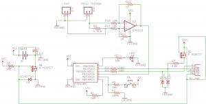
Here is the current schematic.
.
ADC Prescaler / Interrupt
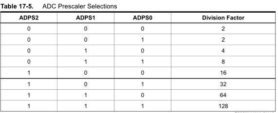
Before we continue, previously I based my assumption of the ADC conversion only taking 65us when at 200KHz however if we use the ATtiny’s internal oscillator for CPU clock speeds (1Mhz, 2Mhz, 4Mhz, etc) there is no ADC clock division / CPU clock combination that will give us 200KHz.
The best we can do is use a division of 8 when at 1MHz to get 125KHz, we multiply the division of 8 by 13 cycles which results in an ADC conversion time of 104us and will give us 9615 samples per second (1 second / 0.000104) . The true samples per seconds will be a bit less than this and we’ll see why when we look at the code later on. The reason I’ve said it will be 13 cycles is because we’ll be using an ADC interrupt which will wake us up when the ADC conversion is complete so it will be a normal conversion taking place.
To use the ADC interrupt we just need to enable the ADIE bit in ADCSRA. Using an ADC interrupt is handy because we want to be able to do other things whilst the ADC conversion is taking place – like writing to the SRAM.
.
Code
Let’s jump into the code; we’ll be re-using some code from the Standalone Temperature Logger.
#define adcPin 3 // Analog input 3
#define ledPin PB0 // Output
int adcMemory[150];
We will log 150 times to the ATtiny’s SRAM
// Wait to be woken up by the ADC interrupt
set_sleep_mode(SLEEP_MODE_ADC); // Set sleep mode ADC
sleep_mode(); // System sleeps here
The sleep mode we’ll be using is ADC sleep mode, if we used the power down mode then the ADC conversion wouldn’t wake us up.
void setup(void) {
  // Change 2MHz to 1 MHz by changing clock prescaler to 16
  CLKPR = (1<<CLKPCE); // Prescaler enable
  CLKPR = (1<<CLKPS2); // Clock division factor 16 (0100)

  sei(); // Turn on interrupts

  // Set ADC prescale factor to 8. (1 MHz clock / 8 = 125 KHz, inside the desired 50-200 KHz range)
  sbi(ADCSRA, ADPS1);
  sbi(ADCSRA, ADPS0);

  // Select ADC3 and 1.1V voltage reference
  ADMUX = (1 << 7) | (adcPin & 0x3f);
}
Nothing unusual in our setup function, we select the ADC3 and 1.1v reference.
// Pin change interrupt
ISR(PCINT0_vect) { }

// ADC conversion complete interrupt
ISR(ADC_vect) { }
The interrupts we use is the pin change and ADC, notice both are left blank which means we’ll just be using them to wake us up from sleep.
int main (void) {
  ...
  while(1) {
    system_sleep();

    int adcResult = 0;
    int adcCount = 0;
    uint8_t adcLowbyte, adcHighbyte;

    // Turn on LED and ADC
    PORTB |= (1<<ledPin);
    sbi(ADCSRA, ADEN);
    sbi(ADCSRA, ADIE);
We go to sleep and wait for a button press before we start logging. When the button is pressed we set up our variables, switch on the ADC and the ADC interrupt.
// Start the ADC conversion
sbi(ADCSRA, ADSC);

// Wait to be woken up by the ADC interrupt
set_sleep_mode(SLEEP_MODE_ADC); // Set sleep mode ADC
sleep_mode(); // System sleeps here

// Log ADC 150 times
while (adcCount < 150) {
  // Read ADC bytes
  adcLowbyte = ADCL;
  adcHighbyte = ADCH;

  // Combine the bytes
  adcResult = (adcHighbyte << 8) | adcLowbyte;

  // Start the ADC conversion
  sbi(ADCSRA, ADSC);

  // Write the previous ADC result to memory
  adcMemory[adcCount] = adcResult;
  adcCount++;

  // Wait to be woken up by the ADC interrupt
  set_sleep_mode(SLEEP_MODE_ADC); // Set sleep mode ADC
  sleep_mode(); // System sleeps here
}
Next start the ADC conversion and go to ADC sleep. When the ADC conversion is complete we are then woken and loop 150 times in which we read the ADC low/high byte and begin the ADC conversion. Whilst the ADC is operating we combine the low/high byte, immediately start the next ADC conversion and write the combined results of the last ADC conversion to the SRAM then we go to ADC sleep.
We’ll wake up and that’s when we read the low/high byte again and re-start another conversion, etc. So you see there is a slight delay from when an ADC interrupt would occur and when we re-start the ADC conversion, it might be 3-8 clock cycles (at 1MHz) but we’ll test this out later.
// Turn off LED and ADC
PORTB &= ~(1<<ledPin);
cbi(ADCSRA, ADSC);
cbi(ADCSRA, ADEN);
cbi(ADCSRA, ADIE);

// Increase clock speed to 16MHz
CLKPR = (1<<CLKPCE); // Prescaler enable
CLKPR = 0; // Clock division factor 1 (0000)

// Transfer the data to the PC
startUSB();
transferData();

// Decrease clock speed to 1MHz
CLKPR = (1<<CLKPCE); // Prescaler enable
CLKPR = (1<<CLKPS2); // Clock division factor 16 (0100)
After we’ve finished the logging, we turn off the LED/ADC and then transfer the logged data to the PC. Download the code here: SACL_v0.1
.
Conversion of logged value to current drawn
int value = adcMemory[eepromAddress];
int baseline = 13; // 13 * 0.001074 = ~14mV baseline
double calculateDouble = ((double) (value - baseline) * 0.01074);

// Split the value into 2 parts
int beforeDecimalpoint = (int) calculateDouble; // Before the decimal point
int afterDecimalpoint = (int) ((calculateDouble - beforeDecimalpoint) * 1000); // After the decimal point

// Fixes incorrect rounding after decimal point
bool insertNumberzero = false;
if (afterDecimalpoint < 100) {
  insertNumberzero = true;
}
The way we calculate the current being used is firstly multiple the result by subtracting the result from the baseline (in my case it was 14mV so I’ve entered this in manually) and then multiplying by 0.01074 (1.1v/1024 * 10) to give us the current being used by the load. Like in the SATVL, we split the values up into the before and after decimal point and have a fix for incorrect rounding.
An example would be that our op-amp is outputting 28mV and the baseline was 14mV. The ADC result would be 0.028mV / 0.001074 = 26 and our baseline result would read 0.014mV / 0.00107 = 13. Next we minus 26 by 13 and multiply by 0.001074 to give us 0.013962 and then we multiply by 10 to give us 0.13962mA which is the current being used by the load. (In the above code, I just multiple by 0.01074 instead of 0.001074 to save an extra step)
.
Simulation of code in AVR Studio
Now we’ll simulate our code in AVR Studio 4 to see how long it would really take to switch on the ADC interrupt after the ADC conversion finished so we can find our real samples per second.
We firstly open the main.elf file.
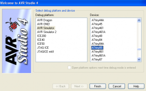
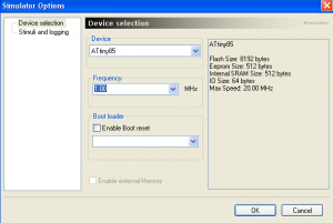
And select ATtiny85 in the simulator options.
We need to change the default clock from 4MHz to 1MHz by going to Debug -> AVR Simulator Options.
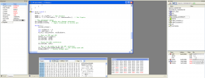
Here is what the simulator looks like. Important keys are:
F5 – Run
Ctrl + F5 – Break
F9 – Toggle breakpoint
F10 – Step over
F11 – Step into
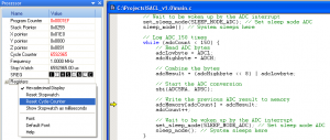
We’ll press F11 a few times and can see it progressing through our code until it reaches the sleep() function and it will stay there forever.
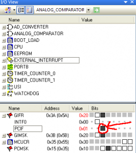
We need to wake up from sleep, first we hit Break. Over in the IO view we click on External Interrupt then near the bottom we see the registers, click on the PCIF register box which will simulate a button press and then press F11 to keep progressing through the code.
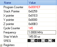
Once we get to the next instruction after starting the ADC we’ll reset the cycle counter so once we get back to the same spot we know how many microseconds have passed.
The microseconds per each ADC conversion, putting the result in SRAM and restarting the ADC takes 145us. The true samples per second of this simulation would be 6,896 (1 second / 0.000145) and with the 10% -/+ of the ATtiny’s internal oscillator of this gives us between 6,206 to 7,585 samples per second.
.
Data from tests
Now we can put our code to the test, below are the results for a static 390 ohm, 1.5k, 2.2k and 10k load.
| 390 Ohm | 1.5K | 2.2K | 10K |
|---|---|---|---|
| 7.507 | 2.137 | 1.514 | 0.332 |
| 7.507 | 2.158 | 1.471 | 0.311 |
| 7.528 | 2.158 | 1.471 | 0.332 |
| 7.507 | 2.158 | 1.492 | 0.332 |
| 7.485 | 2.158 | 1.492 | 0.332 |
| 7.507 | 2.158 | 1.471 | 0.354 |
| 7.485 | 2.158 | 1.492 | 0.354 |
| 7.507 | 2.158 | 1.492 | 0.311 |
| 7.507 | 2.137 | 1.492 | 0.311 |
| 7.485 | 2.158 | 1.492 | 0.332 |
| 7.507 | 2.158 | 1.514 | 0.354 |
| 7.507 | 2.137 | 1.492 | 0.332 |
| 7.485 | 2.158 | 1.492 | 0.311 |
| 7.507 | 2.137 | 1.514 | 0.332 |
| 7.507 | 2.158 | 1.492 | 0.332 |
| 7.485 | 2.158 | 1.492 | 0.311 |
| 7.485 | 2.158 | 1.514 | 0.332 |
| 7.485 | 2.158 | 1.492 | 0.354 |
| 7.507 | 2.158 | 1.514 | 0.332 |
| 7.507 | 2.158 | 1.492 | 0.332 |
| 7.507 | 2.148 | 1.492 | 0.332 |
| 7.507 | 2.137 | 1.492 | 0.332 |
| 7.485 | 2.158 | 1.471 | 0.332 |
| 7.464 | 2.137 | 1.492 | 0.332 |
| 7.464 | 2.137 | 1.492 | 0.332 |
| 7.507 | 2.158 | 1.492 | 0.332 |
| 7.485 | 2.158 | 1.449 | 0.332 |
| 7.507 | 2.137 | 1.514 | 0.332 |
| 7.507 | 2.137 | 1.492 | 0.332 |
| 7.507 | 2.158 | 1.471 | 0.332 |
| 7.507 | 2.137 | 1.492 | 0.311 |
| 7.485 | 2.137 | 1.492 | 0.332 |
| 7.507 | 2.158 | 1.492 | 0.332 |
| 7.485 | 2.137 | 1.492 | 0.332 |
| 7.507 | 2.137 | 1.492 | 0.311 |
| 7.507 | 2.158 | 1.492 | 0.332 |
| 7.507 | 2.158 | 1.492 | 0.332 |
| 7.528 | 2.158 | 1.492 | 0.332 |
| 7.485 | 2.158 | 1.482 | 0.354 |
| 7.485 | 2.18 | 1.492 | 0.332 |
| 7.507 | 2.137 | 1.449 | 0.311 |
| 7.507 | 2.158 | 1.492 | 0.332 |
| 7.485 | 2.158 | 1.471 | 0.332 |
| 7.507 | 2.158 | 1.492 | 0.311 |
| 7.507 | 2.158 | 1.492 | 0.332 |
| 7.507 | 2.158 | 1.492 | 0.332 |
| 7.507 | 2.158 | 1.492 | 0.311 |
| 7.507 | 2.18 | 1.492 | 0.354 |
| 7.528 | 2.137 | 1.492 | 0.332 |
| 7.507 | 2.158 | 1.492 | 0.354 |
| 7.507 | 2.158 | 1.514 | 0.311 |
| 7.507 | 2.158 | 1.514 | 0.354 |
| 7.507 | 2.137 | 1.492 | 0.332 |
| 7.507 | 2.158 | 1.471 | 0.332 |
| 7.507 | 2.158 | 1.492 | 0.354 |
| 7.507 | 2.158 | 1.492 | 0.332 |
| 7.507 | 2.137 | 1.471 | 0.332 |
| 7.507 | 2.158 | 1.492 | 0.332 |
| 7.507 | 2.18 | 1.492 | 0.354 |
| 7.507 | 2.137 | 1.492 | 0.311 |
| 7.507 | 2.137 | 1.492 | 0.311 |
| 7.507 | 2.137 | 1.492 | 0.332 |
| 7.507 | 2.137 | 1.492 | 0.332 |
| 7.507 | 2.158 | 1.492 | 0.332 |
| 7.507 | 2.158 | 1.492 | 0.332 |
| 7.507 | 2.158 | 1.492 | 0.332 |
| 7.507 | 2.137 | 1.449 | 0.332 |
| 7.507 | 2.137 | 1.492 | 0.332 |
| 7.485 | 2.158 | 1.492 | 0.332 |
| 7.507 | 2.137 | 1.492 | 0.332 |
| 7.507 | 2.148 | 1.471 | 0.322 |
| 7.507 | 2.158 | 1.514 | 0.332 |
| 7.528 | 2.158 | 1.492 | 0.311 |
| 7.507 | 2.158 | 1.492 | 0.322 |
| 7.507 | 2.137 | 1.492 | 0.332 |
| 7.485 | 2.115 | 1.492 | 0.311 |
| 7.507 | 2.137 | 1.471 | 0.322 |
| 7.507 | 2.137 | 1.471 | 0.332 |
| 7.528 | 2.158 | 1.492 | 0.332 |
| 7.507 | 2.18 | 1.471 | 0.311 |
| 7.528 | 2.158 | 1.492 | 0.311 |
| 7.507 | 2.158 | 1.492 | 0.332 |
| 7.507 | 2.158 | 1.492 | 0.332 |
| 7.507 | 2.158 | 1.492 | 0.332 |
| 7.485 | 2.148 | 1.492 | 0.332 |
| 7.485 | 2.158 | 1.471 | 0.332 |
| 7.464 | 2.158 | 1.492 | 0.332 |
| 7.507 | 2.158 | 1.471 | 0.332 |
| 7.507 | 2.158 | 1.471 | 0.322 |
| 7.528 | 2.137 | 1.471 | 0.311 |
| 7.507 | 2.158 | 1.492 | 0.354 |
| 7.507 | 2.158 | 1.492 | 0.354 |
| 7.507 | 2.148 | 1.471 | 0.332 |
| 7.528 | 2.18 | 1.471 | 0.332 |
| 7.507 | 2.158 | 1.492 | 0.332 |
| 7.507 | 2.137 | 1.471 | 0.311 |
| 7.507 | 2.137 | 1.514 | 0.332 |
| 7.485 | 2.137 | 1.492 | 0.332 |
| 7.528 | 2.158 | 1.492 | 0.332 |
| 7.507 | 2.158 | 1.492 | 0.332 |
| 7.507 | 2.158 | 1.492 | 0.332 |
| 7.485 | 2.18 | 1.514 | 0.332 |
| 7.507 | 2.18 | 1.492 | 0.332 |
| 7.485 | 2.158 | 1.492 | 0.332 |
| 7.485 | 2.158 | 1.514 | 0.332 |
| 7.485 | 2.18 | 1.449 | 0.332 |
| 7.485 | 2.158 | 1.492 | 0.332 |
| 7.507 | 2.158 | 1.492 | 0.332 |
| 7.507 | 2.137 | 1.471 | 0.332 |
| 7.507 | 2.137 | 1.514 | 0.332 |
| 7.507 | 2.158 | 1.492 | 0.332 |
| 7.507 | 2.158 | 1.514 | 0.311 |
| 7.485 | 2.158 | 1.471 | 0.332 |
| 7.507 | 2.18 | 1.492 | 0.332 |
| 7.507 | 2.158 | 1.492 | 0.332 |
| 7.507 | 2.158 | 1.492 | 0.311 |
| 7.485 | 2.158 | 1.492 | 0.311 |
| 7.507 | 2.201 | 1.492 | 0.332 |
| 7.507 | 2.158 | 1.514 | 0.332 |
| 7.507 | 2.158 | 1.492 | 0.332 |
| 7.507 | 2.158 | 1.492 | 0.311 |
| 7.485 | 2.158 | 1.492 | 0.332 |
| 7.507 | 2.18 | 1.492 | 0.332 |
| 7.485 | 2.158 | 1.492 | 0.332 |
| 7.464 | 2.137 | 1.514 | 0.332 |
| 7.507 | 2.137 | 1.471 | 0.332 |
| 7.507 | 2.137 | 1.514 | 0.332 |
| 7.507 | 2.137 | 1.492 | 0.332 |
| 7.507 | 2.158 | 1.492 | 0.332 |
| 7.485 | 2.158 | 1.492 | 0.332 |
| 7.485 | 2.158 | 1.471 | 0.311 |
| 7.55 | 2.18 | 1.492 | 0.332 |
| 7.464 | 2.137 | 1.492 | 0.332 |
| 7.507 | 2.18 | 1.492 | 0.354 |
| 7.507 | 2.137 | 1.492 | 0.332 |
| 7.485 | 2.137 | 1.492 | 0.332 |
| 7.507 | 2.148 | 1.514 | 0.332 |
| 7.485 | 2.158 | 1.492 | 0.332 |
| 7.485 | 2.158 | 1.471 | 0.332 |
| 7.507 | 2.137 | 1.471 | 0.332 |
| 7.485 | 2.158 | 1.492 | 0.311 |
| 7.485 | 2.158 | 1.492 | 0.311 |
| 7.485 | 2.158 | 1.492 | 0.343 |
| 7.485 | 2.158 | 1.492 | 0.289 |
| 7.507 | 2.137 | 1.492 | 0.311 |
| 7.485 | 2.158 | 1.492 | 0.332 |
| 7.507 | 2.137 | 1.471 | 0.332 |
| 7.507 | 2.158 | 1.471 | 0.332 |
| 7.55 | 2.18 | 1.492 | 0.343 |
.
We know that our resolution is 10uA however our accuracy isn’t as good as I thought it would be, on average it fluctuates and by subtracting the highest value from the lowest value the worst I’ve seen it be is around 90uA accuracy.
Now for a real use situation for the load I hooked up an ATtiny85 with an LED blinking on and off every 1 millisecond.
| 0.848 |
|---|
| 0.869 |
| 1.342 |
| 1.492 |
| 1.471 |
| 1.492 |
| 1.471 |
| 1.471 |
| 1.471 |
| 0.912 |
| 0.891 |
| 0.891 |
| 0.891 |
| 0.869 |
| 0.869 |
| 1.235 |
| 1.492 |
| 1.471 |
| 1.492 |
| 1.471 |
| 1.449 |
| 1.449 |
| 0.934 |
| 0.869 |
| 0.869 |
| 0.869 |
| 0.891 |
| 0.912 |
| 1.063 |
| 1.449 |
| 1.406 |
| 1.406 |
| 1.406 |
| 1.406 |
| 1.406 |
| 0.966 |
| 0.891 |
| 0.869 |
| 0.912 |
| 0.848 |
| 0.848 |
| 0.869 |
| 1.406 |
| 1.385 |
| 1.385 |
| 1.385 |
| 1.385 |
| 1.385 |
| 1.353 |
| 0.955 |
| 0.891 |
| 0.848 |
| 0.848 |
| 0.869 |
| 0.869 |
| 0.998 |
| 1.363 |
| 1.385 |
| 1.385 |
| 1.385 |
| 1.385 |
| 1.385 |
| 0.955 |
| 0.859 |
| 0.869 |
| 0.869 |
| 0.869 |
| 0.912 |
| 0.837 |
| 1.385 |
| 1.374 |
| 1.342 |
| 1.385 |
| 1.385 |
| 1.363 |
| 1.031 |
| 0.912 |
| 0.869 |
| 0.869 |
| 0.848 |
| 0.848 |
| 0.869 |
| 1.342 |
| 1.385 |
| 1.385 |
| 1.363 |
| 1.385 |
| 1.363 |
| 1.063 |
| 0.869 |
| 0.869 |
| 0.891 |
| 0.891 |
| 0.869 |
| 0.869 |
| 1.342 |
| 1.385 |
| 1.385 |
| 1.342 |
| 1.385 |
| 1.385 |
| 1.17 |
| 0.869 |
| 0.848 |
| 0.869 |
| 0.848 |
| 0.859 |
| 0.869 |
| 1.321 |
| 1.363 |
| 1.385 |
| 1.406 |
| 1.406 |
| 1.385 |
| 1.363 |
| 0.869 |
| 0.891 |
| 0.891 |
| 0.869 |
| 0.891 |
| 0.88 |
| 1.321 |
| 1.428 |
| 1.449 |
| 1.449 |
| 1.428 |
| 1.449 |
| 1.449 |
| 0.912 |
| 0.869 |
| 0.869 |
| 0.869 |
| 0.912 |
| 0.891 |
| 1.278 |
| 1.471 |
| 1.471 |
| 1.492 |
| 1.482 |
| 1.449 |
| 1.471 |
| 0.934 |
| 0.891 |
| 0.869 |
| 0.869 |
| 0.869 |
| 0.869 |
| 1.213 |
| 1.471 |
.
I also had my multimeter hooked up to measure the current of the whole circuit which after a few seconds it settled on 1.12 to 1.13mA. If we average our results above, we come to 1.145mA which is very close so it’s a success. Also you will notice that there is 7 results that go high (1.x) and 6 results that go low (0.x), if we divide 1 millisecond by 7 we get 142us (or by 6 gives 166us) which is close to our simulated ADC conversion time of 145us.
For the next part I’ll look into expanding the SRAM to an external SRAM via SPI so we can log more that 150 results.
