So I’ve been able to read/write to a Gameboy cartridge so the next step is emulating one using an Arduino. I wasn’t be able to emulate the whole cartridge using my current methods but I did emulate the cartridge sending the Gameboy the Nintendo Logo. I’ll show you how we can analyse the data coming from the Gameboy and the various steps I went through to get it working.
Let’s jump to the Youtube video straight away to see the results.
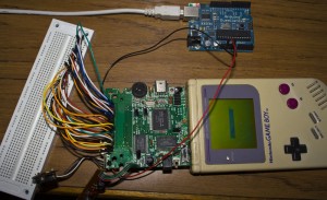
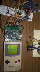
The first thing required is a Gameboy that we can solder some wires to; the Gameboy that I took the cartridge header from was perfect for this and then just place those wires into a breadboard.
Now we all know that when you turn on the Gameboy the Nintendo logo scrolls to the middle of the screen. If no cartridge is inserted it turns on all pixels where the Nintendo logo should be.
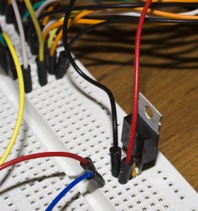
I didn’t want to keep powering the Gameboy from the Arduino so I used a LM7805 regulator to power it.
Logic analyse the Gameboy address lines and clock
Our next step is to find out when the Gameboy requests the Nintendo logo and for that we have our Scanalogic2 device rated at 20MHz; the Gameboy’s CPU is 4.19MHz so our logic scanner will work fine with it. We’ll connect the probes to CLK, A0, A1, A2 then turn the Gameboy on to see what we find. I’m choosing the clock (CLK) specifically to check how fast the clock actually goes.
What’s going on here? This stumped me, a 4MHz CPU should have a clock as 250 250nanoseconds(ns) (1,000 / 4MHz) but I was seeing as short as 75ns and it was varying a lot too!
Something about it didn’t look right so I decided to do a capture at 500KHz which would capture data for 500ms (milliseconds). This brought something to light; it showed the data we got before at the start but then what seemed to be more data towards the middle.
I reset to capture after 100ms and I got something that seemed to have a more stable clock. It seemed to me that perhaps the first data we saw when the Gameboy was turned on might have been some noise.
When you view the whole thing as one it appeared to have some pattern to it so I decided that I had something. The clock was at 400ns which seemed a little slower compared to the real 250ns it should be achieving. Another thing to note is that the shortest on or off time for A0 was actually 800ns, double the clock. So I’m thinking that we could ignore the clock all together and just focus on the address lines.
Reading 8 address lines using the Arduino
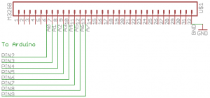
Now it’s time to connect up the Arduino to the Gameboy. I connected up the A0-A7 Gameboy address lines to the Arduino’s D2-D9 pins for simplicity as it gives us an 8 bit number, it was more for a test if I could read the pins properly.
Source1 is the code if you would like to take a look however it’s very basic and for now we are more interested in the data collected. Basically it just waits for anything to come from serial, waits until the address lines are high then delays 50 milliseconds to combat the “noise” above that we saw, logs the data read and then outputs it all to the serial once done.
…
11100011 - 227
00100100 - 36
11111011 - 251
11111011 - 251
11111101 - 253
11111011 - 251
11111010 - 250
11111001 - 249
01111010 - 122
11111111 - 255
11111011 - 251
11011011 - 219
11111001 - 249
11111010 - 250
11111011 - 251
11111011 - 251
…
Above is a shortened version of the data we got, view the whole data here: Read1.

Picture courtesy from GBDev
The Nintendo logo address is 104h (260 decimal) to 133h (307 decimal) and since I didn’t bother with connecting A8 up when we find the number 4 (260 – 256), then 5 (261 – 256) and 6, etc then we know the Gameboy is requesting the logo. We don’t see that in the data above, it all kind of looks like randomness. I then thought about how what we write in the Arduino IDE does more than what we tell it to do and perhaps by using digitalRead it might have been doing more things than just reading the pin?
Manipulating the registers for even faster pin reading
int digitalRead(uint8_t pin)
{
 uint8_t timer = digitalPinToTimer(pin);
 uint8_t bit = digitalPinToBitMask(pin);
 uint8_t port = digitalPinToPort(pin);

 if (port == NOT_A_PIN) return LOW;

 // If the pin that support PWM output, we need to turn it off
 // before getting a digital reading.
 if (timer != NOT_ON_TIMER) turnOffPWM(timer);

 if (*portInputRegister(port) & bit) return HIGH;
 return LOW;
}
Turns out I was right. By looking into C:\Program Files\arduino-0021\hardware\arduino\cores\arduino\wiring_digital.c we can see all the things it does before actually reading the pin.
Next I wanted to test out how long it took to turn a digital pin on and then off again using digitalWrite. I found it to take 5 microseconds (us) to turn on and then off again. That seemed high considering the Arduino runs at 16MHz and we need to take less than 800 nanoseconds (0.8 ns) to read each pin, how can we do this?
After a bit of research it seems that Port Manipulation is the way to go. With the well documented page on the Arduino website, it shows how we can control the ATmega’s port registers directly. This means we could read digital pins 0 to 7 quickly, i.e all in one go (but we shouldn’t as pins 0 and 1 are used for serial communication).
void setup() {
  DDRD |= B00000100; // Set digital pin 2 as an output
}

void loop() {
  PORTD = B00000100; // Turn on digital pin 2
  PORTD &= ~B00000100; // Turn off digital pin 2
  delay(2);
}
Now I wanted to test out to see how fast we can actually turn a pin on and off so it’s back to the logic analyser and by using the simple code above we are able to set digital pin 2 on and off as quick as possible.
One clock cycle of 16MHz is 62.5ns and we can see that its 100ns so about 1.5 clock cycles, that is 50x faster than digitalWrite. Remember that we aren’t just switching it on but are switching it off too which would take another clock cycle which I think is why we are seeing 100ns instead of just 62.5ns. The picture above shows 75ns per division.
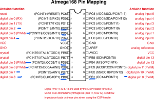
Picture courtesy from Arduino.cc
We can start to look at reading the pins directly now but because the ATmega is divided into different “Ports” and we need to use Ports D and B (shown with blue marker). Ports D are defined as PDx and Ports B are PBx, we will use PD2-8 and PB0-1 which correspond to digital pins 2 to 7 and pins 8 to 9 respectively which is shown in the picture above in red.
byte addressLines = ((PINB << 6) | (PIND >> 2));
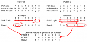
Above is a one liner that will read only the pins that have data which are digital pins 2 to 7 (Port D) and digital pins 8 to 9 (Port B). We will remove the unwanted data by using bit shifting left and right appropriately and using OR to add the bits together as shown above. Now we want to get a definite answer to how long will it take to read both Port D and B.
Find the exact clock cycles for some code
We can find a definite answer for how many clock cycles will take by looking at the de-compiled file which is shown assembly code, finding the instructions used when reading both ports and look at the ATmega328 datasheet to see how many clock cycles it takes for each specific instruction found in the assembly code.
On the Arduino software, hold shift, click compile and it will show you where the temporary compiled files are being stored. Navigate to that directory and then copy over the .elf file to C:\Program Files\arduino-0021\hardware\tools\avr\bin.
avr-objdump.exe -S filenamehere.cpp.elf > asm.txt
Run the above command and a file called asm.txt will be created.
byte addressLines = ((PINB << 6) | (PIND >> 2));
 b0:    83 b1           in    r24, 0x03    ; 3
 b2:    89 b1           in    r24, 0x09    ; 9
Now we just find the part that relates to reading PORT D and B. There is 1 instruction called “in” that’s used twice (notice that it doesn’t do any bit shifting or the OR).
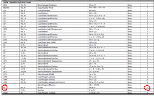
Looking at the ATmega328 summary datasheet on page 13 it says that each “in” instruction takes 1 clock cycle, so it will only take just 2 clock cycles to complete the read of both PINB and PIND.
byte addressLines = ((PINB << 6) | (PIND >> 2));
 bc:    93 b1           in    r25, 0x03    ; 3    1 Clock
 be:    89 b1           in    r24, 0x09    ; 9    1 Clock
 test = addressLines;
 c0:    86 95           lsr    r24    1 Clock
 c2:    86 95           lsr    r24    1 Clock
 c4:    92 95           swap    r25    1 Clock
 c6:    99 0f           add    r25, r25        1 Clock
 c8:    99 0f           add    r25, r25        1 Clock
 ca:    90 7c           andi    r25, 0xC0    ; 192    1 Clock
 cc:    98 2b           or    r25, r24        1 Clock
 ce:    90 93 00 01     sts    0x0100, r25    2 Clocks
The moment you start to do anything with the data it becomes much more than just 2 clock cycles, it seems that before it didn’t do the bit shift or the bit OR, this time it does. I’ve added the clocks next to each instruction above; the total is 11 clocks or 687.5ns (62.5ns x 11). You will soon start seeing how we really don’t have much clock cycles to play around with, imagine when we have to do if statements, while loops, etc. 687.5ns is still under the suspected 800ns that I think the Gameboy might operate at.
Analyse A0-A7 address lines
Now we have to actually store the data we into an array so we can analyse it once it’s finished doing its thing, here I’ll show some code.
byte addrarray[1500];
int addrcounter = 0;

void setup() {
  Serial.begin(57600);
  DDRD |= B00000000; // D2 - D7 input
  DDRB |= B00000000; // D8 - D9 input
}
We set-up Port D and B with all pins as inputs (0) but we will only really use data from pins D2 – D7 and D8 – D9.
void loop() {

  // Wait for serial input
  while (Serial.available() <= 0) {
    delay(200);
  }
  Serial.flush();
  addrcounter = 0;

  byte addressLines = PIND >> 2;
  while (addressLines == 0) {
    addressLines = PIND >> 2; // Only read address lines A0-A6 as others aren't needed
    if (addressLines > 0) { // Hit the noise
      delay(50);
    }
  }
We wait until the we type anything into the serial window and hit enter. Then we read only D2-D7 pins, wait until they aren’t 0 which means the Gameboy has just been turned on and then delay 50ms to skip the noise that happens at 1ms.
 while (addressLines & 1 == 1) {
    addressLines = PIND >> 2;
  }
Now from my testing, the real data starts between 100ms to 150ms but we can’t really tell when unless we keep checking one of the address lines. We keep checking the A0 line and if it’s high we continue in the while loop as from our logic analysing before we found that A0, A1, A2 lines all stay high. Eventually the A0 line will drop to low and that’s when we will begin logging some data.
  while (addrcounter < 1500) {
    addressLines = (PINB << 6) | (PIND >> 2);
    addrarray[addrcounter] = addressLines;
    addrcounter++;
  }

  // Print out
  for (int x = 0; x < addrcounter; x++) {
    for (int z = 7; z >= 0; z--) {
      if (bitRead(addrarray[x], z) == HIGH) {
        Serial.print("1");
      }
      else {
        Serial.print("0");
      }
    }
    Serial.print("\t");
    Serial.println(addrarray[x], DEC);
  }
}
We just read the pins and store them in the array and then print them out after the array is full. Download the code here: Read2
…
00010001 - 17
00010001 - 17
…
01000111 - 71
01000111 - 71
00000100 - 4
00000100 - 4
00000100 - 4
00000100 - 4
11111101 - 253
11111100 – 252
…
11111101 - 253
11111101 - 253
11000101 - 197
00000101 - 5
00000101 - 5
00000101 - 5
00000101 - 5
11111101 - 253
11111100 - 252
…
11111101 - 253
11111101 - 253
00000110 - 6
00000110 - 6
00000110 - 6
00000110 - 6
00000110 - 6
11111100 - 252
11111100 - 252
…
View the full data here: Read2. Are you starting to see a pattern? It’s starting to look like it’s counting starting from 4 then going to 5, then to 6… before I said “if we find the number 4 (260 – 256), then 5 (261 – 256) and 6, etc then we know the Gameboy is requesting the logo” so I think we may have it!
  while (addrcounter < 1500) {
    while (addressLines >= 250) { // Ignore this data
      addressLines = (PINB << 6) | (PIND >> 2);
    }
    addressLines = (PINB << 6) | (PIND >> 2);
    addrarray[addrcounter] = addressLines;
    addrcounter++;
  }
But let’s be absolutely sure; let’s add a simple statement to ignore any value over 250 as it kind of seems these are everywhere and might not matter to us. Updated code for download: Read3
…
01000111    71
01000111    71
01000100    68
00000100    4
00000100    4
00000100    4
11111101    253
00000101    5
00000101    5
00000101    5
00000101    5
11111100    252
00000110    6
00000110    6
00000110    6
00000110    6
11111100    252
00000111    7
00000111    7
00000111    7
00000111    7
11111100    252
…
11111101    253
00110010    50
00110010    50
00110010    50
11111101    253
00110011    51
00110011    51
00110011    51
00111101    61
11111100    252
01000010    66
Full data here: Read3. That looks much cleaner, so we have 4 as the starting address and 51 as the end address. Add A8 bit as high (+256) for each and then convert to hex and that does give us 104h and 133h, we definitely have found the request for the Nintendo Logo!
Re-analysing the data
Remember how I said we need to be under 800ns? Well it turns out that our new data doesn’t support this theory, it shows that we could potentially take a few microseconds because the 4, 5, 6, etc values came up 3 times in our data and we know that our capturing of the Port D/B will take at least 700ns but with while loops and storing to the array maybe it’s already up to 1000ns (1us). Let’s see if we can compare the data we captured to the logic analyser data.
All we need to do is look for small changes in A0, A1 and A2 that might indicate that the address is being sent out. Seems like there is a longer delay on the left part of the picture verus the right part. The 1 2 3 4 5 in the picture indicates the similarities.
After analysis of the longer delay at 20MHz with A0 A1 A2 A3 lines, it appears that time period that these lines are actually used for data is for 4.8us, so it seems we have a longer time to do things and this is the reason that we are seeing the 4, 5, 6, etc numbers appear 3 times in our data.
Writing the Nintendo Logo
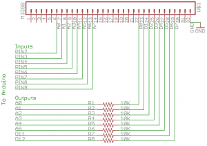
Now that we have enough data to go off, we’ll need to actually write data to the D0-D7 pins on the Gameboy. We will use the Arduino’s analog pins 0 to 5 for D0-D5 and the Arduino’s digital pins 11-12 for D6-D7. This means that we’ll be using more and more clock cycles but since we have the newly suspected 4.8us to play around with it shouldn’t be a problem.
// The nintendo logo
byte nintendoLogo[48] = {0xCE, 0xED, 0x66, 0x66, 0xCC, 0x0D, 0x00,
0x0B, 0x03, 0x73, 0x00, 0x83, 0x00, 0x0C, 0x00, 0x0D, 0x00, 0x08,
0x11, 0x1F, 0x88, 0x89, 0x00, 0x0E, 0xDC, 0xCC, 0x6E, 0xE6, 0xDD,
0xDD, 0xD9, 0x99, 0xBB, 0xBB, 0x67, 0x63, 0x6E, 0x0E, 0xEC, 0xCC,
0xDD, 0xDC, 0x99, 0x9F, 0xBB, 0xB9, 0x33, 0x3E};

void setup() {
  DDRD |= B00000000; // D2 - D7 as inputs (on GB reads A0-A5)
  DDRB |= B00011000; // D8 - D9 as input (on GB reads A6-A7), D11 - D12 as outputs (on GB writes D6-D7)
  DDRC |= B00111111; // A0 - A5 as outputs (on GB writes D0-D5)
}
We insert the nintendo logo in an array to be easily accessible. As before we have the setup of the PORT pins but this time with DDRB (Port B) we set Arduino pins 11 and 12 as outputs. We also add DDRC (Port C) which are the analog pins 0 to 5 and set them as outputs too.
void loop() {

  byte addressLines = PIND >> 2;
  while (addressLines == 0) {
    addressLines = PIND >> 2; // Only read address lines A0-A6 as others aren't needed
    if (addressLines > 0) { // Hit the noise
      delay(50);
    }
  }
We have the start of the loop and hit the noise part like before.
  boolean readyToOutput = false;
  while (addressLines != 68) { // Indicates the end of reading the header
    while (addressLines >= 250) { // Ignore this data as it's not related to the header
      addressLines = (PINB << 6) | (PIND >> 2);
    }

    // Read the address lines A0-A8
    addressLines = ((PINB << 6) | (PIND >> 2));
Now if you really looked into the full data of Read3, you would have noticed that after the number 51 there was a constant number 68 that keep coming up, once we hit that number we know we are finished so we have a while loop to filter it out. After that it’s the same as before.
    if (addressLines == 4) { readyToOutput = true; }

    // Start at position 0 on in nintendoLogo array
    if (addressLines >= 4 && addressLines <= 51 && readyToOutput == true) {
      PORTC = nintendoLogo[addressLines-4];
      PORTB = ((nintendoLogo[addressLines-4] & 192) >> 3);
    }
  }

  // Turn off outputs
  PORTC = 0;
  PORTB &= ~B00011000;
}
Now what we do is check for the “start condition” of 4 (+256 dec = 104h) because in Read3 there are numbers like 17, 18, 36, etc which would all be valid numbers and we don’t want to output anything until we hit 4. When we hit 4, we set the boolean to true and if the number read is between 4 and 51, it’s real data. To map this data input to our array which starts at 0 we minus 4 from it, easy.
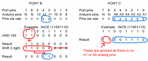
To turn on the outputs we use PORTC = x, if we were writing 0xCE it would be like writing PORTC = B11001110 which would turn on outputs A1-A3 as high. For PORTB it’s a little bit tricky, we actually only want the 2 MSB (2 left bits) so we AND it with 192 (11000000) then shift 3 bits right so that those two bits that we did the AND with will align to on Arduino D11 and D12.
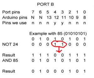
After it’s all done, we turn off all outputs in PORTC and PORTB. PORTB is special as we don’t want to touch any other bits other than D11 and D12 because we are using D9 and D10 as inputs. By using NOT (~B00011000) we flip the bits specified so it’s like writing B11100111 and then use AND to safely turn off D11 and D12 without affecting the other pins. Now lets try it out on the Gameboy, download the code here: Write 1
Hmm, we have something displayed on the Gameboy but it doesn’t look correct. I can sort of see an N for the Nintendo, but some parts of it don’t align up properly. Maybe my analysis of 4.8us was incorrect? I thought now what I would do is actually output each element of the Nintendo logo array before the request as it seemed like the top left place was always left blank, this means we would be outputting 0xCE before it even wrote the number “4”.
  if (addressLines > 0) { // Hit the noise
    delay(50);
  }
}

PORTC = nintendoLogo[addressLines-4];
PORTB = ((nintendoLogo[addressLines-4] & 192) >> 3);
So what we’ll do is after we hit the noise, we add it to output the first element of the nintendo logo array.
// Start at position 1 on in nintendoLogo array
if (addressLines >= 4 && addressLines <= 51 && readyToOutput == true) {
  PORTC = nintendoLogo[addressLines-3];
  PORTB = ((nintendoLogo[addressLines-3] & 192) >> 3);
}
Now we just change this part to start at the second element of the array and that’s all the changes needed. Download it here: GB_Nintendo_Logo_Emulate_v1.0. Now lets give it a try…
It works!
Re-analyse 1 address line with 1 output line
So obviously my analysis of 4.8us was incorrect, so I wanted to see what the real time was and for that it’s back to the logic analyser. This time however we tweak the delay of the output such that we can pin point the precise moment that the Gameboy reads the D0-D7 pins.
The above was what we were doing before we applied the fix, as you can see it takes us 2.2us to process the address and write to the outputs.
After lots of testing and tweaking the delay, we can see that it’s 800ns total. So the first 400ns seems to be for the Gameboy to send real data to address lines and the next 400ns is for the Gameboy to read the data. This means we need to do everything that we were doing in that 2.2us in 800ns now, which doesn’t seem possible with our current methods.
PORTC = nintendoLogo[addressLines-3];
 ea:    86 95           lsr    r24
 ec:    86 95           lsr    r24
 ee:    e2 95           swap    r30
 f0:    ee 0f           add    r30, r30
 f2:    ee 0f           add    r30, r30
 f4:    e0 7c           andi    r30, 0xC0    ; 192
 f6:    e8 2b           or    r30, r24
 f8:    f0 e0           ldi    r31, 0x00    ; 0
 fa:    e3 50           subi    r30, 0x03    ; 3
 fc:    ff 4f           sbci    r31, 0xFF    ; 255
 fe:    80 81           ld    r24, Z
 100:    88 b9           out    0x08, r24    ; 8
Just to show you why it’s not possible in this current method, when just assigning PORTC with the nintendo loop array variable takes at least 12 clock cycles – 750ns.
void loop() {
 PORTC = nintendoLogo[PIND];
 b8:    89 b1           in    r24, 0x09    ; 9
 ba:    e0 e0           ldi    r30, 0x00    ; 0
 bc:    f1 e0           ldi    r31, 0x01    ; 1
 be:    e8 0f           add    r30, r24
 c0:    f1 1d           adc    r31, r1
 c2:    80 81           ld    r24, Z
 c4:    88 b9           out    0x08, r24    ; 8
}
However if we could find a microcontroller that has for example, PORTC and PORTD as 8 unused pins continuously, then we might stand a chance with the above code at 8 clock cycles – 500ns but just from loading data from the SRAM.
Conclusion
So what did we learn?
- You have to keep refining your theories on how things work
- Use port manipulation for faster writing/reading of pins
- How to find out how many clock cycles a specific piece of code takes
- Even when you are trying to emulate something with a faster clock speed it can still be difficult
- With the ATmega328 clocked at 16MHz, all the different PORTs for the pins, the shifting of bits required, there isn’t a clear way we can read the address lines and write to the data lines under 800ns
- You would need a faster microcontroller with 16 pins for the address lines (if you want full cartridge emulation) and 8 for the outputs (preferably with 3x PORTs with 8 unused pins for each) and with the ability to communication quickly to a EEPROM or Flash device
So I hope this has been quite informative and that you have learnt something from it, I sure did when doing all of this! I think that emulating the whole cartridge is a bigger job than it seems, although I’m happy that at least writing the Nintendo logo was achievable 🙂









This is brilliant work. Ive been wanting to emulate a cartridge on the gameboy for some time now and your articles have given me the inspiration to give this a try. So maybe an arduino isn’t fast enough but do you think it might be possible with another atmega with the right amount of pins and a suitable crystal?
Keep up the good work!
Thanks! It might be possible to do with an atmega (like 164A, 324A, 644A, 1284A, etc) with 40 pins as they have dedicated pins for the crystal and have 4 x PORTs (0-7), the main limitation is that the AVR range only runs at 20MHz max as far as I can see. 20Mhz vs 16MHz over 400ns would give you about 1 more clock cycle to play around with.
Now if you have 50MHz that would give you 13 more clock cycles which is very nice. There is also the atxmega is clocked at 32MHz and the UC3 32bit processors are at 50-66MHz depending on the one you get. There is also another chip that someone else is using for doing a Gameboy cart flasher called the parallax propeller which seems to have 8 processors and could run at 80mhz which seems very interesting.
If we assume 400ns as the worst case scenario, after the Gameboy has written to the address lines, you might have a interrupt to detect it and then you have about 400ns to process it and then output the data. Now what I didn’t do was get past the logo so you never know maybe it’ll become faster or slower than 400ns.
Good luck and let me know how you go 🙂
Hello,
just one remark: DDRB |= B00000000; does absolutely nothing (the same thing applies to some other places where you are using “|=”), because “|=” sets all bits in DDRB which are also set in B00000000, i.e. none. If you want to set all pins at port B to inputs, you have to use “=” (or “&=”) instead of “|=”.
Best regards,
CherryDT
Hello,
Has any further progress been made with this? I’m very interested by this project!
Hi Andres, unfortunately I haven’t put any more time into this project. I figured that emulating the logo was good enough for me 🙂 but I’m sure there are better options that I haven’t explored like using an ARM uC.
Awesome stuff, I was wondering if an AVR was fast enough to emulate an MBC. This answers that!. I’ll give it a try with an ARM uC. I’ll post the results up on my site soon. http://www.Bennvenn.com/mx.html
[…] logic devices, either CPLDs or FPGAs to handle the high-speed logic requirements. [Alex] proved that a microcontroller could emulate a cartridge by using an Arduino to display the “Nintendo” Game Boy boot logo. The […]
[…] logic devices, either CPLDs or FPGAs to handle the high-speed logic requirements. [Alex] proved that a microcontroller could emulate a cartridge by using an Arduino to display the “Nintendo” Game Boy boot […]
[…] logic devices, either CPLDs or FPGAs to handle the high-speed logic requirements. [Alex] proved that a microcontroller could emulate a cartridge by using an Arduino to display the “Nintendo” Game Boy boot […]
[…] Emulating the Nintendo Logo on the Gameboy […]
It’s probably late in the day, but, the noise you were seeing was probably down to reading/writing regardless of the state of the CS line.
Hi Alex.
I’m trying to manipulate something similar in Sega Master System. It is very difficult to get guindance from people with experience like yours.
I’m late, you may not even be focused on developing this project anymore. Sorry for this, I am in a country where access to certain knowledge is late.
I subscribed to your YouTube channel and put your sites as my favorites.
My goal is to create a Flash Cart for Sega master System console. But I have several barriers to overcome.
Any Arduino has a severe SRAM memory limitation. So, we can’t build byte arrays that are over 29 Kb on Arduino Uno and Arduino Mega, there’s just a little more memory. Perhaps, an ESP32 might perform better on this. I don’t know.
But, Alex, have you tried a process like what I will suggest next? We create a txt file, containing bytes in hexadecimal format . We put this file on SD card. We use Arduino to read this hex data through an SD module and print to the serial port. So, we create the following array for writing: byte data [] = {Serial.read ()}; .
I’m researching if this would work , a friend suggested to me.
If this is possible, we can avoid “array overflow” issues in Arduino boards.
Does it work?
Everything you produce is amazing. From your content to your products for sale.
Best Regards.
Hi Dan,
That method may work however timing would be very important depending on what the application is, if it’s just to emulate a logo then timing can be worked on. For a flash cart, the problem is the device can request to read any piece of data and you have to respond then and there most of the time.
Many flash carts that use an SD card usually transfer the SD card rom to a flash chip and then start the rom from the flash chip, so you’d need to write a little loader to do this – perhaps that could sit in the Arduino’s memory. Otherwise you could always just put a flash chip on your cart and use the Arduino to write to it while it’s plugged into your PC.
If you haven’t already, you should check out the building a flash cart series as I think a good amount could also apply to other systems: https://www.insidegadgets.com/2018/04/18/building-a-2mb-mbc5-gameboy-cart-part-1-cpld-as-the-mbc-and-adding-flash-as-our-rom/
First of all, I am very grateful that you answered me with such detailed information. Thank you very much! your answer help me a lot.
I will access the link now, at lunch time and I will study this material.
Alex, I’m from Brazil. The game community here in Brazil is today one of the largest in the world. The retro game wave is booming in my country, even with the biggest economic crisis we have ever experienced.
If it is possible for you, try to look for Brazilian companies and offer them the patent for your products. They can manufacture here and sell them for an affordable price. The dollar here is high. Your products are amazing and I think the gamer community will love it.
Best Regards.