As part of my CPLD Logic Analyser project, I might want to easily adjust the clock and since the CPLD that I’m using doesn’t have a PLL module, we’ll have to buy our own clock generator.
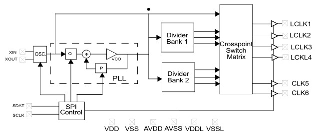
The Cypress CY22150 chip allows you to generate a clock up to 200MHz from a 8-30 MHz crystal using I2C and has multiple outputs / clock dividers. For the price of $2.77 it’s not too bad and for me was actually cheaper than buying a 100MHz crystal from my supplier.
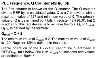
There are a few settings we need to configure – the crystal frequency, crystal capacitors, which outputs to enable and clock multipliers and dividers. This may seem a bit complex at first but Cypress have made a CyberClocks program that can assist us with these settings.
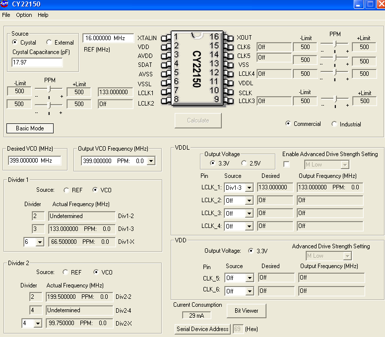
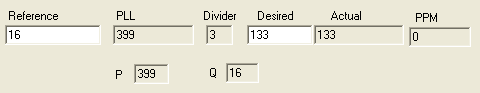
I have a 16MHz crystal, so we enter that on the top left. The VCO is given to us in another section of this program (Option > VCO Calculator) as shown below, I enter in the Reference as the crystal and desired clock as 133MHz.
After we’re given the VCO, the datasheet says we need to select the divider 1 dropdown box as 6 for the divider of 3 to be enabled and shows 133 MHz as we wanted.
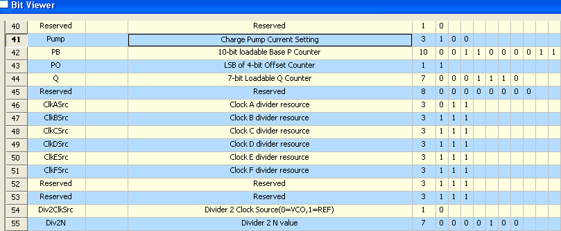
We can now see which bits in each register need to be set, one thing that I found was wrong was the charge pump setting which should really be 001.
.
Understanding each register to be set
Crystal Drive Setting (12H)
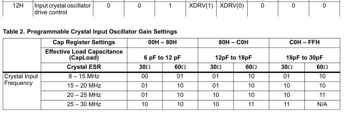
The 16MHz crystal I’m using has an ESR of 50 ohms, so we’ll select 60 ohms, XDRV will be 10 so the register will be 00110000.
Input Load Capacitor Control (13H)
![]()
My 16MHz crystal has a load capacitance of 18pF.
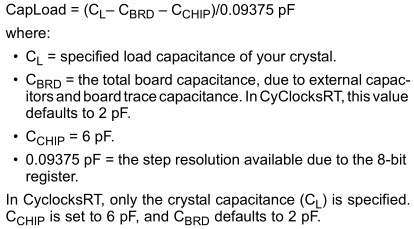
The formula we use is shown above however the Cyberclocks program can automatically calculate the correct 8 bit capacitance needed which in this case was 01101011.
Clock Output Enable Control (09H)
![]()
As I just want 1 output enabled as LCLK_1, we set this register to 1.
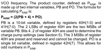
PLL Frequency, Q Counter [42H(6..0)]
![]()
The first step in generating the PLL is the the Q counter which is used for dividing our crystal, in this case our Q counter is 16 which was given to us by Cyberclocks so 16 Mhz / 16 Q = 1 MHz.
Since our Q counter is 16, the minimum Q counter is 2 if we write 0 to this register, so we’ll just need to minus 2 from our 16 so we write 14 to this register, 1110. (PO explained next)
Charge Pump and PB Counter (40, 41H)
![]()
After Q counter, we multiply the result by P which Cyberclocks gave us a value of 399.
We calculate Ptotal by using the formula above. In our case to generate 399 Ptotal, we do: 2 x (195 + 4) + 1.
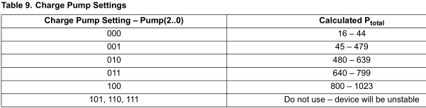
For the charge pump setting since out Ptotal is 399, we can use 001. Our registers will look like: 11000100 (40H) and 11000011 (41H). Since we need PO to be 1, we have to set this in 42H which now will read 10001110.
DIV1SRC Mux and DIV1N Divider (0CH) and Crosspoint Switch Matrix Control (44, 45, 46H)
![]()
Now that we have the 399MHz for the PLL, we’ll have to say that we want to use the PLL, so we set DIV1SRC to 0, otherwise our clock will come from the crystal directly.
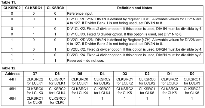
We need to divide our PLL by 3 to give us 133MHz, so we’ll need to set CLKSRC1 and CLKSRC0 to 1. Each clock output has it’s own divider too, as we are only interested in LCLK1 then 44H will be 01100000. As we used the fixed /3 divider it says we need to set DIV1N to 6, so 0CH will be 00000110.
.
Testing
// General crystal setup and output enable
soft_i2c_write_byte(DEVICE_ADDR, 0x12, 48); // 16 MHz, 60 ohm ESR
soft_i2c_write_byte(DEVICE_ADDR, 0x13, 107); // Crystal capacitance control for 18pF crystal
soft_i2c_write_byte(DEVICE_ADDR, 0x09, 1); // Enable LCLK_1 output

// 133 MHz
soft_i2c_write_byte(DEVICE_ADDR, 0x0C, 6); // Select VCO with 6 divider (For fixed /3 divider option, set DIV1N to 6)
soft_i2c_write_byte(DEVICE_ADDR, 0x44, 96); // LCLK_1 set to DIV1CLK/3
soft_i2c_write_byte(DEVICE_ADDR, 0x42, 142); // PO = 1 and Q = 16 (14 value + 2)
soft_i2c_write_byte(DEVICE_ADDR, 0x40, 196); // Charge pump = 2 (P total = 45 – 479)
soft_i2c_write_byte(DEVICE_ADDR, 0x41, 195); // PB value = 195 (for P total 399)
I’m using an ATtiny85 to write to the registers, Download ATtiny85_CY22150
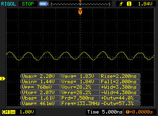
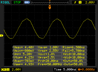
My 50MHz scope does show 133MHz though to be honest it was jumping around between 131 to 135 MHz but I believe this is because of the 50MHz scope, the breadboard and wires; measuring 50MHz works ok too.
It seems to work well and it’s a easy part to use once you understand how it operates.


I need circuite for Cypress CY22150 Programmable Clock Generator
and outher documents.
Is there any IC which can provide stable digital clock pulses …. In my project I need a circuit / IC which can give me stable clock pulse from 5khz to 50khz (in this range) . Currently I’m using uc2825 ic for clock pulse generation but that ic drops the frequency of pulses if starting pulse frequency is 26 khz then after 5min it will become 25khz…I need stable clock generator please tell me….
Hey Darshan,
look on your datasheet, maybe you have to hold your VCO in a given frequency range. In the datasheet from the cypress 22150 it is between 100MHz and 400MHz to work correctly.
I hope that helps you 🙂