Previously we made a SNES transmitter board which allows you to converter your SNES controller to a wireless controller and allow you to use any of the existing receivers we have available.
Today we’ll look at making an NES drop in board for the generic NES controllers you can buy off Ebay and also revisit the GBA TX cart’s CPLD code after I made a basic 32MB GBA cart so we can remove the 50 MHz oscillator.
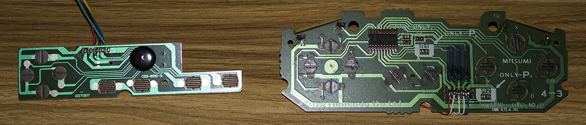
It seemed like a good starting point for the drop-in boards as the existing board shape is pretty simple where as the SNES board shape is a bit more complex.
(sneak peak, new boards will be ordered)
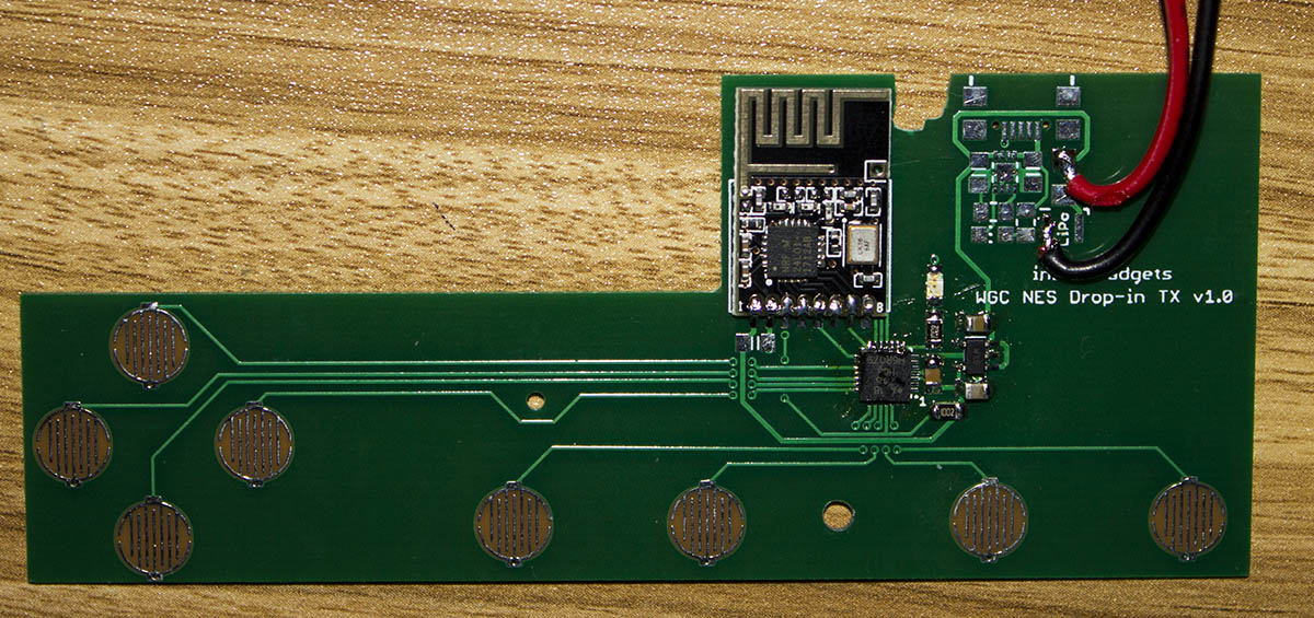
We can pretty much re-use all the components we used on the SNES TX mod board for this NES drop in board. Now that we’ll have control of the buttons ourselves we don’t have any chip that we need to switch on with a P mosfet and thus our power consumption when sleeping and power on response when the start button is pressed will be improved.
The only thing I hadn’t done before was making button pads on the PCB before. I looked around for existing Eagle libraries that had them but only found one which was pretty small. There are lots of different designs out there, some like the SNES have carbon coated pads on the PCB and others just have the bare PCB exposed.
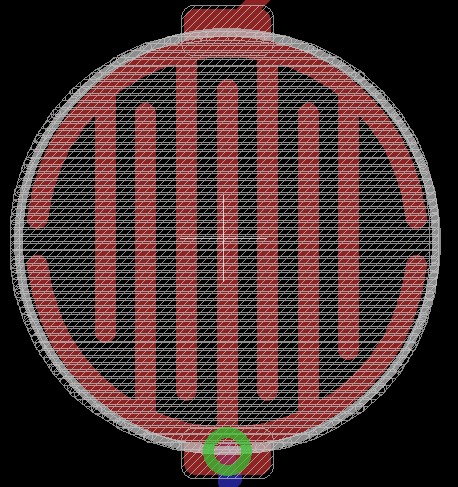
I made my own design which was basically a copy of PCB pad I had seen online, lots of traces close enough that any conductive material when pressed on it should short it out. I’d probably make the traces a bit more wider, maybe 0.3mm instead of 0.254mm.
After settling on the buttons, I spent a while just measuring out the board, measuring the existing button placements, figuring out where I could mount the USB connector and the nRF24 wireless module, it came together good enough.
For the button detection, we can just use the pull-up resistors found on the ATtiny48 and connect the other button side to ground and we save ourselves 8 resistors. When no button is being pressed, the pin state is high, exactly the same as the NES/SNES controllers work.
// Power down nRF24 and MCU
if (inPowerDown == 1) {
	PORTD &= ~(1<<LED);
	NRF_POWERDOWN;
	PCICR |= (1<<PCIE1); // Enable interrupt to wake us up
	system_sleep();

	PCICR &= ~(1<<PCIE1); // Disable interrupt
	inPowerDown = 0;
	NRF_TX_POWERUP; // Power up to transmitter mode
	_delay_ms(5);
	PORTD |= (1<<LED);
}

// Clear existing data
kpData[0] = 0;

// Check buttons
if (!(PINC & (1<<BUTTON_UP))) { // Up
	kpData[0] |= 0x10;
}
As you can imagine, there isn’t much going on in the code, just the usual go to power down sleep routine and as mentioned before we don’t have to wake up every 8 seconds to check key presses as we can just assign the pin change interrupt on the start button. Once the start button is pressed, we wake up, check the key presses and transmit the packet until the start button is held for 5 seconds or a 5 minute timeout, then MCU goes back to sleep.
I mustn’t have measured the board thickness correctly as I ordered 0.8mm where as the existing board was 1.6mm which actually does make a difference in terms of the direction keys – seems it’s very easy to activate the up/down keys if you press the left/right keys in a certain way, I would have thought it would be the opposite. Adding a 0.8mm board to the back helps this issue, so I’ll be sure to order 1.6mm boards.
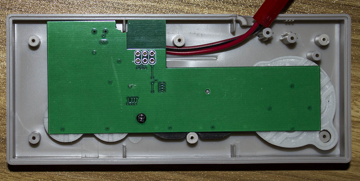
One problem with the NES controller is that there really isn’t much room for a battery, I had a 160mAh battery which just fit under the board.
32MB Dev Cart
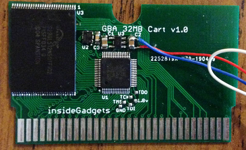
While it’s not directly related to this product, one user did query me about making a GBA flash cart and since I had already laid out a GBA 32MB flash cart (no save capability) a month or two after completing the GBA TX cart, I thought why not just order it as see how it goes. I was just able to swap out the 4MB MX29LV160 to the 64MB S29GL512 which is used in the Gameboy 64MB Mighty Flash Cart and just re-route some traces (technically you could switch between 2x 32MB games by toggling A24). I’ll have to make a new revision of the board as the flash chip is blocking the top of the case from closing, plus I’ll add a couple of pins broken out from the CPLD too.
Once receiving the board, I just loaded up the same CPLD code that the GBA TX used and thought it should all be fine. I was indeed able to erase the flash chip, write 32MB and read back 32MB ok however when trying out certain games, even if they didn’t have save capabilities, some wouldn’t work past the Nintendo logo which was a bit confusing.
I decided I would try to use the block schematic editor instead of Verilog to put together the logic elements myself. This wasn’t the first time using the block schematic editor before, back when creating the GBA TX cart, I tried to make a duplicate of the GBA flash cart schematic someone created but that didn’t work out, couldn’t fit on the chip – there were errors about the “fan-out” from what I recall.
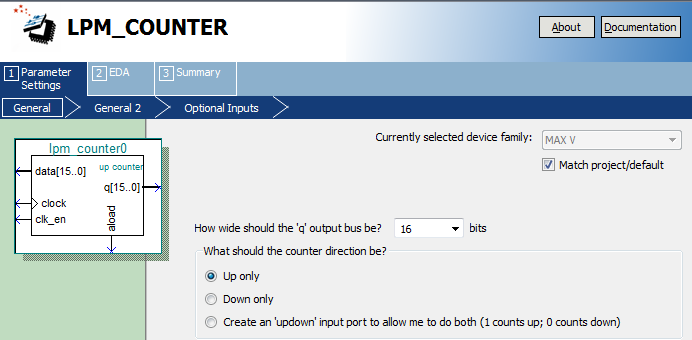
This time I was looking through all the logic elements and noticed that there was an Altera megafunction lpm_counter which as it suggests is just a counter which you can make as many bits as you like – for us, we are after 16 bits. There are other options as well such as clock enable, carry-in, carry-out, synchronous and asynchronous clear, load or set.
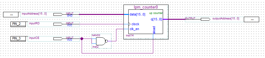
We need the clock to connect to the RD line so the counter will increment when RD is pulsed but not before the clock is enabled which is done by setting CE low and latching the address presented on A0-A15. For the latching, we enable asynchronous load which when the pin is high it loads the address – so every time CE stays high, the address keep on being loaded until CE goes low.
I compiled it and it fit without any issues. Programmed the CPLD and gave it a test running a 32MB ROM video player game, seemed like the best thing to try, lo and behold it worked first try! This means we are running without the need of the 50MHz oscillator which is used on the GBA TX cart.
Revisiting the GBA TX cart
So I thought why not try this on the GBA TX cart, the only issue is we’ll have to make the following in the schematic: Store 7 data bits when WR goes low, set a pin high for a certain amount so the AVR knows data is ready and then set the pin low again.
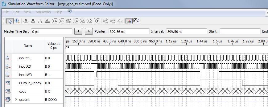
Unfortunately it didn’t work first time, it took many attempts to figure out what was going on plus the logic didn’t behalf like I thought it should. There is a handy Simulation Waveform Editor which allows you to set pins at certain intervals high/low and acting as a clock, etc which really does help when troubleshooting logic. Take a look at this video on how to get started with it.
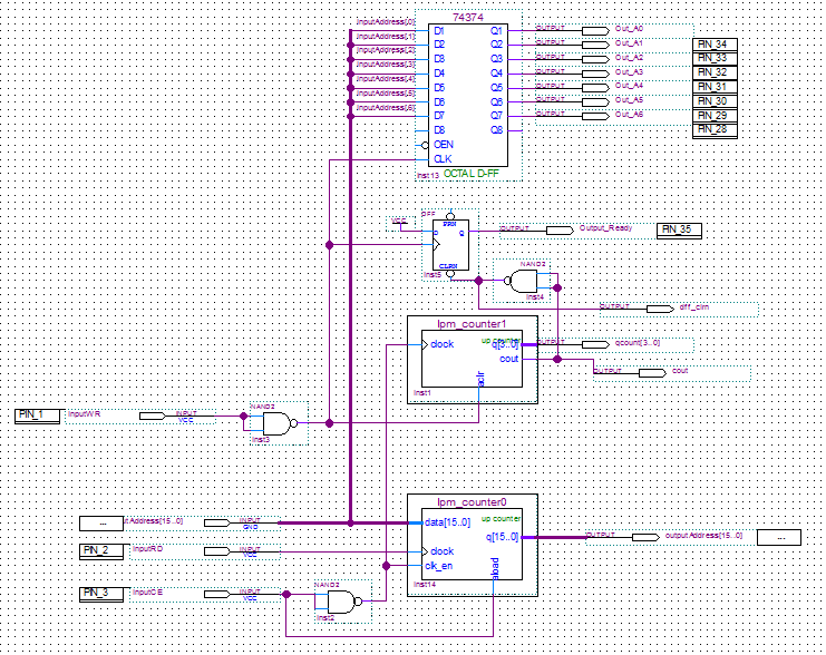
With a bit of trial and error, I came up with a schematic that works. Once WR goes low, the NAND gate outputs a high signal which clocks the 74374 DFF and the data is now stored. It also clocks the single DFF which sets the output ready signal as high. The AVR receives that signal and has a limited time to read that data. That time limit is determined by the bit length of the lpm_counter1 which is 4 bits, it too was reset when WR was pulsed.
Every pulse of CE then forth will increment the counter until it reaches 1111 which should then reset the single DFF output ready to low and restart the counter to 0 again.
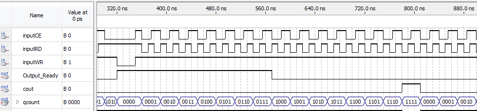
I say should because that’s not quite what I’m seeing in the waveform and that’s really odd. It actually resets at 1000 but yet I still can see the cout output test pin pulse high at 1111. I wonder why this might be?
And this would probably be considered a very simple schematic but it’s a little bit complex, though I do like the feel of modifying logic like this. It does appear that you may be able to write some Verilog and combine it with your schematic as a module, that something I might have to look into.
I’ll give everything a bit more of a test and then I no longer need to add in the 50MHz oscillator to the board.


