From the last part, we switched to the CH340G USB to serial converter which gave our read speeds a bit of a boost, we looked at reading the GBA ROM, SRAM reading/writing and how to automatically determine ROM/SRAM sizes. In this part, we’ll cover EEPROM read/write, Flash writing and determining EEPROM size and checking if we have SRAM or Flash.
I was previously looking at the ATmega32A which I’ve received and was able to switch to, it has just enough pins, with 2 pins to spare, one will be an LED pin and the other will detect the 5V/3.3V switch so we know whether we’ll be interfacing with the GB or GBA.
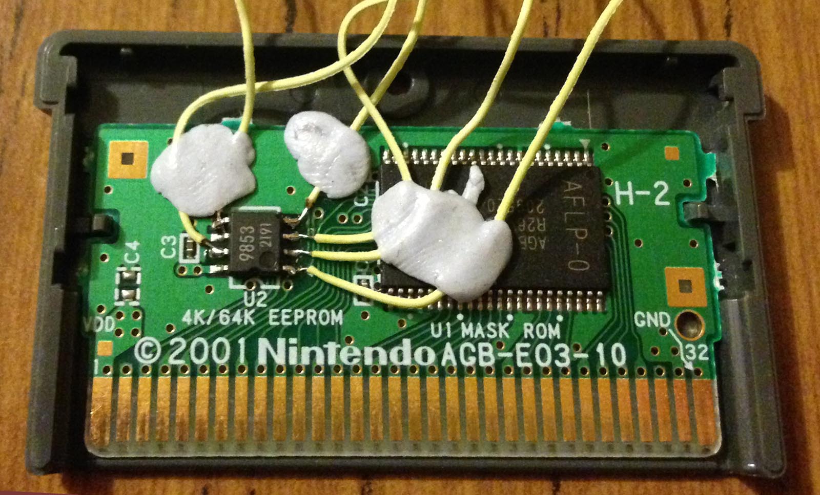
On to the EEPROM, I found the GBATek page which gives a explanation on how to address the EEPROM and what to do when reading/writing so it’s a good and simple resource to use though I wanted to see for myself how the GBA interfaced with EEPROM with any timings I need to consider. I broke out the logic analyser on the Fila Decathlon game which uses a 4Kbit EEPROM.
Writing to EEPROM
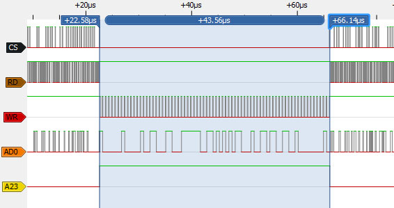
Thankfully the game allows you to save to the EEPROM after the first event so I was on my way. For a write, we can see that CS goes low, RD goes high, WR is the clock line as we drive the EEPROM serially, AD0 is the data and A23 goes high. If we were to read from the EEPROM, the RD pin would be the clock and the WR pin would be high.
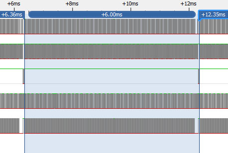
Just to see what an expanded view looks like, the GBA seems to wait 6ms before writing again, around the standard waiting time for an EEPROM write.
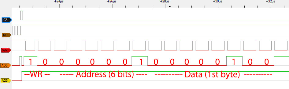
Let’s go through how we address and write data to the EEPROM in finer detail by reference of the GBATek information. First we send a write request (10), then the 6 bit address in this example the address is 1 and the first data byte. We continue to send another 7 bytes and end the write request with an end bit as 0 (not shown). The clock frequency is 600ns, not a problem for us.
A 4Kbit EEPROM has 64 addresses (where the 6 bit address comes from) with 64 bit data each and a 64Kbit EEPROM has 1024 addresses (10 bit, although it seems we need to write 14 bits instead) with 64 bit data. After going through a few of these writes with the logic analyser I could see the address bits increment and eventually saw the name I’d chosen in game.
Reading the EEPROM
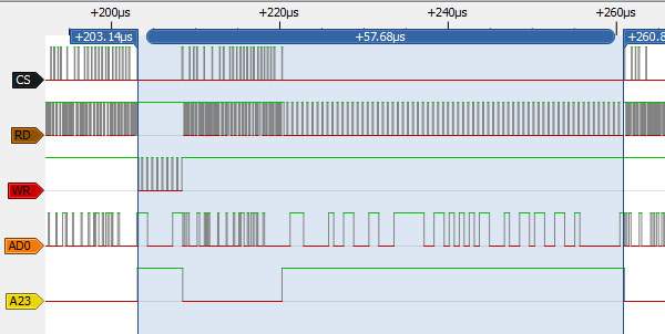
Now we can look at reading from the EEPROM, we see it’s accessed in two steps (A23 goes high), firstly we send the address we wish to read and then read out the 64 bits.
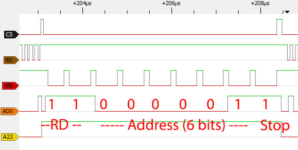
This time we start of with a read request (11), the address we wish to read (1) and the stop bit which should be 0 but I actually found that sometimes the stop bit was 1, in my example above.
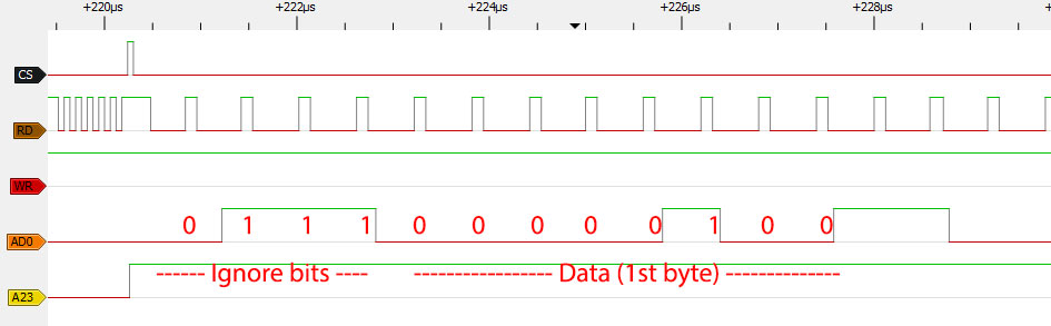
We have to ignore the first 4 bits and then we have the 64 bits of data. We now understand how the EEPROM works, now we have to replicate the reading, writing and addressing in our code.
void gba_eeprom_mode (void) {
	GBA_PORT_ROM_ADDR7_0 = 0xFF;
	GBA_PORT_ROM_ADDR15_8 = 0xFF;
	GBA_PORT_ROM_ADDR23_16 = 0xFF;
}

void gba_eeprom_set_address(uint16_t address, uint8_t eepromSize, uint8_t command) {
	cs_mreqPin_low;

	int8_t x = 0;
	if (eepromSize == EEPROM_64KBIT) {
		...
	}
	else {
		if (command == EEPROM_READ) {
			address |= (1<<7) | (1<<6);
		}
		else {
			address |= (1<<7);
		}
		x = 7;
	}

	// Loop through address, 8 or 16 bits depending on EEPROM
	while (x >= 0) {
		if (address & (1<<x)) {
			ad0Pin_high;
		}
		else {
			ad0Pin_low;
		}

		wrPin_low; // CLK
		asm ("nop");
		asm ("nop");
		wrPin_high;
		asm ("nop");
		asm ("nop");
		x--;
	}

	// Only send last low bit and wr/cs high if reading, as writing is done in 1 continuous chunk
	if (command == EEPROM_READ) {
		ad0Pin_low;
		asm ("nop");
		wrPin_low;
		asm ("nop");
		asm ("nop");

		wrPin_high;
		cs_mreqPin_high;
	}
}
As both writing and setting the address for a read both use the same start (RD/WR bits, 6 or 14 address bits), I decided to combine these starts into one function. We first check if it’s a 4Kbit or 64Kbit EEPROM and set the appropriate bits, then we loop through those bits keeping in mind the clock frequency of 600ns, 2 nops for the high/low clock does the trick and then we send a stop bit only if we are reading (we assume the next function called will do the rest). We don’t need to worry about setting the A23 line high or low as gba_eeprom_mode function sets all pins high for us and gba_mode will be called later to set them all low (not shown).
gba_eeprom_set_address(address, eepromSize, EEPROM_READ);

GBA_PORT_EEPROM_DATA7_0 &= ~(1<<AD0); // Set AD0 pin as input
GBA_DDR_EEPROM_DATA7_0 &= ~(1<<AD0);

cs_mreqPin_low;

// Ignore first 4 bits
for (int8_t x = 0; x < 4; x++) {
	rdPin_low; // CLK
	asm ("nop");
	asm ("nop");
	rdPin_high;
	asm ("nop");
	asm ("nop");
}

// Read out 64 bits
for (uint8_t c = 0; c < 8; c++) {
	uint8_t data = 0;
	for (int8_t x = 7; x >= 0; x--) {
		rdPin_low; // CLK
		asm ("nop");
		asm ("nop");
		rdPin_high;

		if (GBA_PIN_EEPROM_DATA7_0 & (1<<AD0)) {
			data |= (1<<x);
		}
	}
	eepromBuffer = data;
}

cs_mreqPin_high;
If we were reading, here’s how it would all look. After setting the address, we ignore the first 4 bits and then loop the 64 bits, after each 8 bits are read place that byte on the array.
gba_eeprom_set_address(address, eepromSize, EEPROM_WRITE);

// Write 64 bits
for (uint8_t c = 0; c < 8; c++) {
	for (int8_t x = 7; x >= 0; x--) {
		if (eepromBuffer & (1<<x)) {
			ad0Pin_high;
		}
		else {
			ad0Pin_low;
		}

		wrPin_low; // CLK
		...
	}
}

// Last bit low
ad0Pin_low;
...
Writing is almost the same except that we just send 64 bits of data and then send the stop bit, I followed the advice and set the stop bit to 0. For the PC interface side, it’s similar to reading/writing to the SRAM methods except that we send the EEPROM size at the start and then send or request 8 bytes at a time. After a few tests, everything is working well.
Determine EEPROM Size
We need a way to find out whether an EEPROM is present on the cartridge and if that EEPROM is 4Kbit or 64Kbit. After some tests, if you try to read out an EEPROM from a cartridge that doesn’t have one, it will return 0x00 or 0xFF, so that’s easy, plus I don’t think there would be any carts that woudl have SRAM with an EEPROM, wouldn’t make much sense but you never know. Also it turns out that if you address a 4Kbit EEPROM as a 64Kbit, it repeats the same 8 bytes (64 bits) over and over again.
uint16_t currAddr = 0x000;
uint16_t endAddr = 0x200;
...
while (currAddr < endAddr) {
	com_read_bytes(READ_BUFFER, 8);

	if (currAddr == 0) { // Copy the first 8 bytes to check other readings against them
		memcpy(&firstEightCheck, readBuffer, 8);
	}
	else { // Check the 8 bytes for repeats
		for (uint8_t x = 0; x < 8; x++) {
			if (firstEightCheck[x] == readBuffer[x]) {
				repeatedCount++;
			}
		}
	}

	// Check for 0x00 or 0xFF bytes
	for (uint8_t x = 0; x < 8; x++) {
		if (readBuffer[x] == 0 || readBuffer[x] == 0xFF) {
			zeroTotal++;
		}
	}

	currAddr += 8;

	// Request 8 bytes more
	if (currAddr < endAddr) {
		RS232_cputs(cport_nr, "1");
	}
}
RS232_cputs(cport_nr, "0"); // Stop read

if (zeroTotal >= 512) { // Blank, likely no EEPROM
	return EEPROM_NONE;
}
if (repeatedCount >= 300) { // Likely a 4K EEPROM is present
	return EEPROM_4KBIT;
}
else {
	return EEPROM_64KBIT;
}
So what we’ll do is read the first 8 bytes, store that, then read the rest of the 4Kbit EEPROM size (0x200), check for how many 0x00 or 0xFF we find and also how many repeated bytes we find. If the count of 0x00 / 0xFF is more than 512 then we have no EEPROM, otherwise if the repeated count is more than 300 then we have a 4Kbit EEPROM (sometimes it doesn’t give us a perfect 512 result so I made it a bit lenient).
Writing to Flash
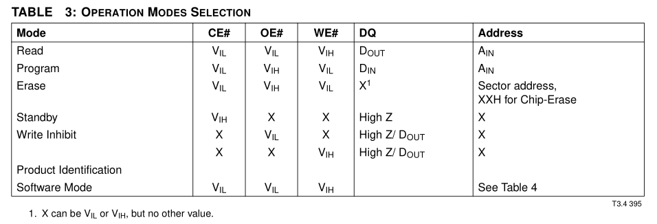
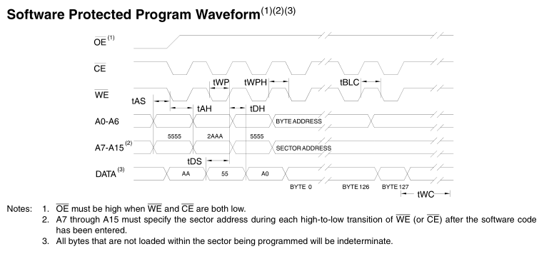
Now it’s time for writing to the flash memory. First thing we need to do is pull up the datasheets (LE39FW512) that are still available and firstly check what pins we need to use. It has CE, OE, WE, the data pins and address pins, similar to SRAM except that in this case OE (output enable) is like RD and WE (write enable) is like WR; they are active low as well as CE.
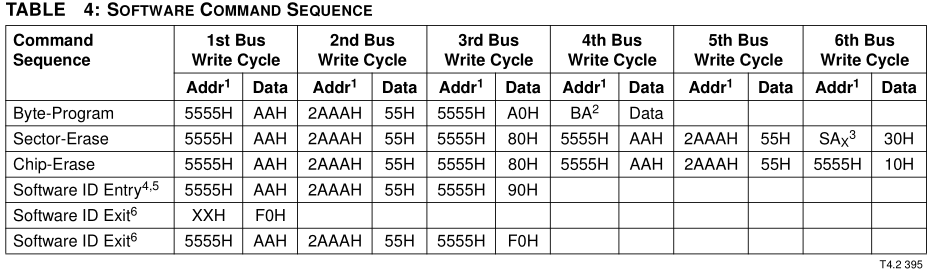
We also need check the sequence we need to perform, as with flash they seem to take extra pre-cautions so there is almost no way you could re-write the flash by mistake. This particular flash chip is written byte by byte (20uS program time), where as some flash like Atmel ones write 128 bytes at a time. Before we can write a byte we have to either perform a sector erase or chip erase, I’ll go for the sector erase which takes 18ms, each sector is 4Kbytes.
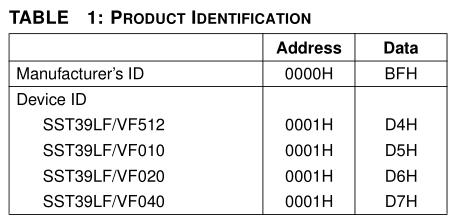
Reading the Software ID (chip ID) will also be useful to know which manufacturer it is but more importantly for us to know if it’s an Atmel chip or not. After reading the software ID, you need another sequence to exit that mode. In order to do any writing, we firstly write to the address 0x5555H with the data 0xAA, set WR and CS2 low, wait a tiny bit and then set WR and CS2 high and continue with the next bus write cycles.
void flash_write_bus_cycle(uint16_t address, uint8_t data) {
	GBA_DDR_RAM_DATA7_0 = 0xFF; // Set data pins as outputs
	set_16bit_address(address);
	GBA_PORT_RAM_DATA7_0 = data;

	wrPin_low;
	cs2Pin_low;
	asm volatile("nop");
	wrPin_high;
	cs2Pin_high;
}
We can simply put this into a function and write to the bus all the times required.
void flash_erase_4k_sector(uint8_t sector) {
	flash_write_bus_cycle(0x5555, 0xAA);
	flash_write_bus_cycle(0x2AAA, 0x55);
	flash_write_bus_cycle(0x5555, 0x80);
	flash_write_bus_cycle(0x5555, 0xAA);
	flash_write_bus_cycle(0x2AAA, 0x55);

	flash_write_bus_cycle((uint16_t) sector << 12, 0x30);
	_delay_ms(25); // Wait 25ms for sector erase
}

"3. SA X for Sector-Erase; uses A MS -A 12 address lines
A MS = Most significant address
A MS = A 15 for SST39LF/VF512, A 16 for SST39LF/VF010, A 17 for SST39LF/VF020, and A 18 for SST39LF/VF040"
To erase a 4K sector, we follow the write cycles, then left shift the sector number by 12 and the data to write is 0x30.
void flash_read_chip_id(void) {
	flash_write_bus_cycle(0x5555, 0xAA);
	flash_write_bus_cycle(0x2AAA, 0x55);
	flash_write_bus_cycle(0x5555, 0x90); // Software ID entry
	_delay_ms(20); // Wait a little (for Atmel chip)

	// Set data as inputs
	GBA_PORT_RAM_DATA7_0 = 0;
	GBA_DDR_RAM_DATA7_0 = 0;

	// Read manufacturer and device ID
	flashChipIdBuffer[0] = gba_read_ram_8bit_data(0x0000);
	flashChipIdBuffer[1] = gba_read_ram_8bit_data(0x0001);

	flash_write_bus_cycle(0x5555, 0xAA);
	flash_write_bus_cycle(0x2AAA, 0x55);
	flash_write_bus_cycle(0x5555, 0xF0); // Software ID exit
	_delay_ms(20); // Wait a little (for Atmel chip)
}
Software ID works similar except that once the entry write cycles are complete, you read from the address 0 and 1 like you would for SRAM and then perform more write cycles to exit Software ID mode.
As mentioned previously, there is one chip that writes different from the others, the Atmel 512Kbit one (AT29LV512). Instead of erasing a sector and writing the bytes, it takes care of it all for us, we send it the sector address and 128 bytes whilst incrementing the byte address. We have 150uS between each byte sent otherwise it will re-program the bytes that it has so far and blank out the rest, that timing won’t be an issue and the write cycle time is 20ms.
void flash_write_sector(uint16_t sector) {
	flash_write_bus_cycle(0x5555, 0xAA);
	flash_write_bus_cycle(0x2AAA, 0x55);
	flash_write_bus_cycle(0x5555, 0xA0);

	// Write the bytes (A0-A6 byte address, A7-A15 sector address)
	for (uint8_t x = 0; x < 128; x++) {
		flash_write_bus_cycle((uint16_t) (sector << 7) | (uint16_t) x, receivedBuffer[x]);
	}
	_delay_ms(20); // Wait sector program time
}
Like the others we write the bus cycles and then send out the 128 bytes, I had to increase the buffer on both ATmega and PC interface to 129 bytes to support this.
void flash_switch_bank(uint8_t bank) {
	flash_write_bus_cycle(0x5555, 0xAA);
	flash_write_bus_cycle(0x2AAA, 0x55);

	flash_write_bus_cycle(0x5555, 0xB0);
	flash_write_bus_cycle(0x0000, bank);
}
We just have one thing left to do which is to support 1Mbit Flash, these have 2 banks as we access it via 16 bit address lines, luckily GBATek had the sequence available as I don’t have a 1Mbit Flash cart handy.
uint32_t readBytes = 0;
for (uint8_t bank = 0; bank < ramBanks; bank++) {
	// Set start and end address
	currAddr = 0x0000;
	endAddr = ramEndAddress;
	set_number(currAddr, SET_START_ADDRESS);

	// Program flash in 128 bytes at a time
	if (hasFlashSave == FLASH_FOUND_ATMEL) {
		while (currAddr < endAddr) {
			com_write_bytes_from_file(GBA_FLASH_WRITE_ATMEL, ramFile, 128);
			currAddr += 128;
			readBytes += 128;

			print_progress(readBytes, 1024, 4096);
			com_wait_for_ack(); // Wait for write complete
		}
	}
	else { // Program flash in 1 byte at a time
		if (bank == 1) {
			set_number(1, GBA_FLASH_SET_BANK); // Set bank 1
		}

		uint8_t sector = 0;
		while (currAddr < endAddr) {
			if (currAddr % 4096 == 0) {
				flash_4k_sector_erase(sector);
				sector++;
				com_wait_for_ack(); // Wait 25ms for sector erase
			}

			com_write_bytes_from_file(GBA_FLASH_WRITE_BYTE, ramFile, 64);
			currAddr += 64;
			readBytes += 64;

			print_progress(readBytes, 1024, 4096);
			com_wait_for_ack(); // Wait for write complete
		}
	}

	set_number(0, GBA_FLASH_SET_BANK); // Set bank 0 again
}
On the PC side when we are re-programming the flash, we loop as many banks required (max 2) and we only want to set the bank once we hit the 2nd bank as the non-1Mbit flash chips may not support the bank change command, for non-Atmel chips we check to see if the current address is a modulus of 4096 and if so, erase the current sector before we write to it, then read 64 bytes from the file as usual; for Atmel chips, we just send it 128 bytes at a time.
Checking to see if we have SRAM or Flash when writing
So we have a little bit of a problem, how do we check to see if we have flash or an SRAM, reading them is the same (apart from if you have a 1Mbit Flash with bank swapping), only writing them is different. If you were to request the Flash Software ID on an SRAM, you would actually be writing to the SRAM with those write cycle data bytes, not good!
// Save the 1 byte first to buffer
uint8_t saveBuffer[65];
set_number(0x0000, SET_START_ADDRESS);
set_mode(GBA_READ_SRAM);
...

// Check to see if the first byte matches our test byte (1 in 255 chance), if so, use the another test byte
uint8_t testNumber = 0x91;
if (saveBuffer[0] == testNumber) {
	testNumber = 0xA6;
}

// Write 1 byte
set_number(0x0000, SET_START_ADDRESS);
uint8_t tempBuffer[3];
tempBuffer[0] = GBA_WRITE_ONE_BYTE_SRAM; // Set write sram 1 byte mode
tempBuffer[1] = testNumber;
...

// Read back the 1 byte
uint8_t readBackBuffer[65];
set_number(0x0000, SET_START_ADDRESS);
set_mode(GBA_READ_SRAM);
...

// Verify
if (readBackBuffer[0] == testNumber) {
	printf("SRAM found\n");

	// Write the byte back to how it was
	set_number(0x0000, SET_START_ADDRESS);
	tempBuffer[0] = GBA_WRITE_ONE_BYTE_SRAM; // Set write sram 1 byte mode
	tempBuffer[1] = saveBuffer[0];
	...

	return NO_FLASH;
}
else { // Flash likely present, test by reading the flash ID
	printf("Flash found\n");

	set_mode(GBA_FLASH_READ_ID);
	com_read_bytes(READ_BUFFER, 2);

	// Check if it's Atmel Flash
	if (readBuffer[0] == 0x1F) {
		return FLASH_FOUND_ATMEL;
	}
	// Check other manufacturers
	else if (readBuffer[0] == 0xBF || readBuffer[0] == 0xC2 ||
		readBuffer[0] == 0x32 || readBuffer[0] == 0x62) {
		return FLASH_FOUND;
	}

	return NO_FLASH;
}
The solution I came up with is basic but a destructive one if done incorrectly, we read the first byte of the SRAM/Flash, then write to that same byte with a choice of 2 bytes (just in case, the byte read is the same one will are about to write with) but the way which we write is like we are using SRAM. We read the byte back, if it matches our written byte then we have SRAM, otherwise we have flash.
Determining Flash size
In our check SRAM/Flash size, we previously checked for SRAM/Flash up to 512Kbit as both are read the same way but for testing 1Mbit flash we have to switch banks.
// Read bank 0
set_number(0, SET_START_ADDRESS);
set_mode(GBA_READ_SRAM);
...

set_number(1, GBA_FLASH_SET_BANK); // Set bank 1

// Read bank 1
set_number(0, SET_START_ADDRESS);
set_mode(GBA_READ_SRAM);
..

set_number(0, GBA_FLASH_SET_BANK); // Set back to bank 0

// Compare
for (uint8_t x = 0; x < 64; x++) {
	if (firstBuffer[x] == secondBuffer[x]) {
		duplicateCount++;
	}
}

// If duplicated bank 0 and 1, then we have 512Kbit Flash
if (duplicateCount == 64) {
	return SRAM_FLASH_512KBIT;
}
else {
	return SRAM_FLASH_1MBIT;
}
So we can just read the first 64 bytes of bank 0, switch to bank 1 and read 64 bytes again and see if they match (This is untested).
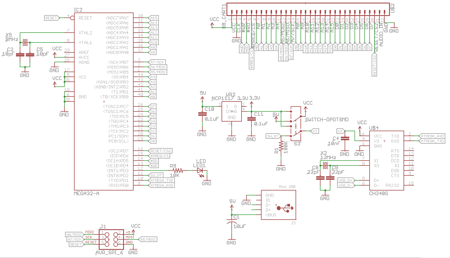
Here’s how the schematic looks, we are almost done. I have the ATmega detect what was the last free pole in the switch, we detect o if CH340G is generating it’s own 3.3V (means it’s 5V Vcc). I don’t have any free pins left for LEDs to show if we are on 3.3V or 5V, I think the easiest solution will be to use an inverter hooked up to the same pole, kind of disappointing that I need that!
Now that we have the switch detect, we can combine the GB/GBA functions into one and query the ATmega to know which one we should use.
All that’s left to do now is layout the PCB and it should hopefully all be good!
GBxCartRead – Part 1: Design and Testing Gameboy Carts
GBxCartRead – Part 2: Switching to CH340G, GBA ROM reading, SRAM read/write and determining sizes
GBxCartRead – Part 3: GBA EEPROM Read/Write & Flash Write and Determining Sizes
GBxCart RW v1.0 Released


Alex,
Thank you so much for using your time to publish this. Very interesting investigation. I will be looking forward to the availability of the PCB layout.
Keep the good work!