In Part 6, we looked at upgrading the Multi-game feature to allow for mixing GB/GBC games by using a hardware reset on the Gameboy plus we added the ability to switch the CPLD to select MBC3 or 1 mode (MBC5 is the default) when using the loader.
One issue I wasn’t able to solve was why the GBP didn’t seem to work with the multi-game loader (it doesn’t work on the “22 in 1” cart either) so we’re going to have a look at that and also look at possibly making a new larger sized flash cart using 3.3V flash.
When trying to boot a game from the multi-game loader, we just receive a blank Nintendo logo. If I perform a manual hardware reset, it resets it back to the loader menu fine.
if (multiStage == 2'd1 && inputAddress == 4'd6) begin
  multiStage <= 2'd2; // Turn off any more multi-game bank changing
  romBankMulti <= 7'd1;
  romBank <= 7'd1;
  ramBank <= 2'b0;
  resetGB <= 1'b0; // Reset Gameboy
It felt like perhaps the bank to switch to wasn’t being set correctly, so I tried manually setting a bank in the CPLD when we triggered the reset and that worked without any issues. This leads me to believe that the GBP isn’t outputting the data fast enough in order for the CPLD to pick up the bank before it resets.
// Second stage - Check address 0x6000-6FFF for the bank to switch to
if (multiStage == 3'd1 && inputAddress == 4'd6) begin
	romBankMulti <= inputData;
end
// Third stage - Check address 0x7000-7FFF for reset
if (multiStage == 3'd2 && inputAddress == 4'd7) begin
	multiStage <= 3'd3; // Turn off any more multi-game bank changing
	romBank <= 7'd2;
        ramBank <= 2'b0;
        resetGB <= 1'b0; // Reset Gameboy
end
So after playing around for a while, I decided to switch back to executing the commands from the HRAM and adding another stage to the loader to do the reset after the multibank variable is loaded.
Unfortunately this didn’t seem to work, the Gameboy never reset. It looks like by reusing the 0x7000-7FFF as the third stage that part doesn’t execute, I even tried to include the clock line into it but no luck. I ended up changing the address to look for to be 0x5000-5FFF and then it worked perfectly, very odd.
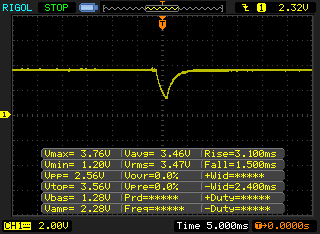
Part of the troubleshooting process was to look at the reset lines after the R/C filters to see how they performed, it looked like they didn’t rise above 3.3V because of the 1.5K resistor I had connected to the CPLD was set as an output as 3.3V. That’s probably not great so I should fix that.
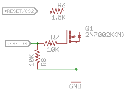
I just added a N mosfet to short the reset line through the 1.5K resistor, so now instead of pulsing the reset GB line to ground, we pulse it high so the mosfet turns on, easy right?
resetGB <= 1'b0; // Reset Gameboy
changed to
resetGB <= 1'b1; // Reset Gameboy
Not quite, it looks like reversing how the resetGB pin is used in all the code caused the system not to reset again!
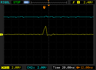
I could see pulse being generated by the CPLD to the mosfet but it only lasted less than 20ns.
// Third stage - Check address 0x5000-5FFF to reboot
if (multiStage == 2'd1 && inputAddress == 4'd5) begin
	...
	resetGBReg <= 1'b0; // Reset Gameboy
end
...
assign resetGB = !resetGBReg;
The work around I came up with was to use a register, use the assign command with a NOT of the register so basically it just outputs the opposite of the register and now it works. Also since the third stage variable didn’t matter, I set it back to just being 2 bits and we save 1 macrocell that way.
Designing a 64MB (3.3V Based) Flash Cart
Since the 2MB 128KB SRAM & 32KB FRAM Flash carts are finished I thought I’d look at designing a larger capacity flash cart, I still want to stick with NOR based flash for the moment. I was looking at having multiple size options – 16MB/32MB/64MB but the price difference between them isn’t that significant, maybe $4-5 so I’m just going for the 64MB flash option which means this cart will need to be a multi-game cart.
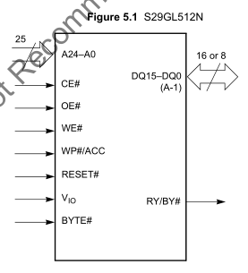
For the flash chip, it looked like the S29GL512N would do the job, it’s just like any other flash chip. It has the option to switch between 8-bit/16-bit modes, it operates on 3.3V but also has a VIO pin that lets you choose the I/O voltage it operates at (1.65V to Vcc), kind of similar to what some CPLDs offer; we’ll just hook it up to Vcc.
Speaking of CPLDs, as we have more address lines to account for so we’ll have to switch to a different CPLD with more IO. I was first looking at the Atera 5M80Z which has 54 IO, it runs at 1.8V so we would need another LDO and allows an IO voltage up to 3.3V.
One thing I didn’t really like about it was the small 0.4mm pin pitch (EQFP-64) plus I was starting to test out 80 LE (64 macrocells “equivalent” version) in the Altera software to see if the Multi-game cart code would fit but it didn’t. It appears that a macrocells in this device aren’t the same as the EPM3064 I used for the 2MB flash carts.
So we’d have to go for the 5M160Z which they also have as a TQFP-100, it has 160 LEs but it’s not really cheap at $7 each (actually the 240 LE version is around the same price). I started searching for old Altera CPLD variants and came across the EPM3128 which offered 128 macro-cells, was a TQFP-100, runs on 3.3V (but isn’t 5V tolerant) and was a few dollars from Aliexpress so I’ve decided to go with it instead.
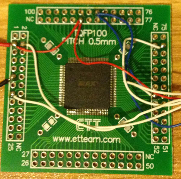
I ordered 10 of them, soldered one on to a breakout board to make sure it would program the chip which it did. It consumes 17mA unprogrammed and 82 macrocells used consumes 73mA.
Since we’re using 3.3V for our flash chip and CPLD we need a way to interface with the 5V that the Gameboy puts out on it’s IO pins. A logic level translation chip is what we need and there are some that allow you to switch which direction the translation will take place (5V input to 3.3V output or 3.3V input to 5V output) by toggling a pin.
The reason we need the direction switching is because when the Gameboy wants to write to the SRAM (or if we wish to write to the flash chip), the WR line goes low and the chip is now reading data that the Gameboy puts on the data lines. The WR line goes high and then RD line goes low to read data from the Flash/SRAM, so we need to switch which direction the data will flow, in or out.
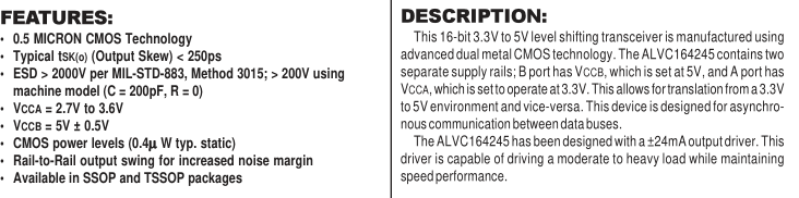
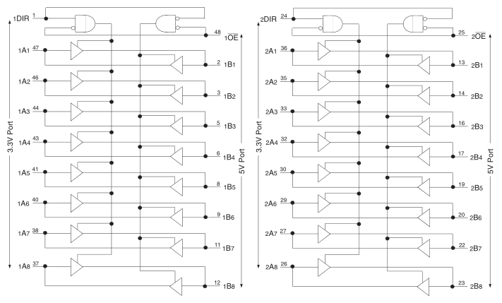
The IDT 74ALVC164245 looks like it will do the job, it has 2 banks of 8 IO per chip and allows for direction switching of each bank, so we’ll need 2 of them. One will cover Clock, RD, WR, CS, A0 to A11 and the other will do A12 to A15, Reset and D0-D7 will be on it’s own bank.
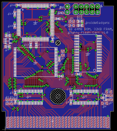
This isn’t really a flash cart I want to wire up by hand, so just when I had some spare time I began laying out the board, a week or so later I was done. It’s been sent to the PCB fab for a prototype so we’ll see how it goes!


