Now it’s time for the part that you and I have been waiting for, the PCB development of this circuit! It sure did take me while to get everything I need for this and a some research on this topic but in the end it all worked out. This is a step by step guide to how to develop your PCB using a collaboration of various resources I’ve found on the net so you should be set to make your own PCB once you have a design after reading this.
First I’ll start off with some acknowledgements of resources I used:
- PCB design: SparkFun Eagle: PCB Layout (they have lots of helpful tutorials and a great range of parts)
- Etchant process – Stop using Ferric Chloride etchant! & Etching with Air Regenerated Acid Cupric Chloride
- PCB development two sided toner method – Two sided PCB using toner method
- PCB development videos – How to make a PCB & PCB Etching, Dying and Tinning
Now for what we’ll need:
- Copper Clad board (FR4 or similar) – can be found on Ebay pretty cheaply, example
- Dremel metal diamond tipped blade (can be found cheaply on Ebay too) and dremel – for cutting out the PCB from the copper clad
- Brasso or Steel wool & Isopropyl alcohol – from a hardware shop or can be found online, for cleaning the PCB
- Laser printer, paper, paper clips and sticky tape – for printing the PCB and aligning layers
- Iron – for transferring the PCB design to the board
- Hydrochloric acid (also named muriatic acid) & Hydrogen Peroxide – from a hardware/pool shop and a chemist/drug store (or you can use ferric chloride), to remove the copper from the PCB
- Glass container, small plastic container, gloves and a plastic clamp – for containing the acid solution, measuring and protection
- A set of drill bits ranging 0.7mm to 1mm and a drill press or dremel mount – for drilling the holes
On to the PCB development process.
PCB design
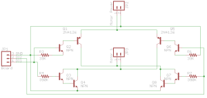
This is the part that takes a long time, up to a few hours easily if it’s your first time. We’ll use a PCB design tool, for example, Eagle from CadSoft. Eagle lets us layout out our components on a board and lets use route the wires connecting them together. Please do view the SparkFun Eagle: PCB Layout to get you started before reading on as I won’t do a full on tutorial on using Eagle. The basics is you firstly design your schematic from components in the libraries provided with Eagle (you can grab more libraries yourself, SparkFun have one too). Be careful when using components, you need to make sure they match you component or check that the pin spacing, size, etc is similar to yours.
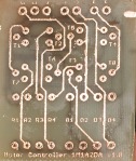
Once you place the components on the schematic you draw the wires connecting them together. After you’ve done that, you create a board from the schematic which places all your components with a “connection” wire on a board. You then move the components to however you like on the board and then draw in the real wires to the board, the “connection” wire is just there to show you which components connect to each other, it’s fairly helpful. The minimum size for the wire connection to use is 0.254mm or 0.1inch (I had to use 0.3mm) and you should avoid using curves or right angles with your wires. The size for text that I find works well is 1mm for the “Motor Controller” text and 0.9mm for the description of pins / parts (“DI1”, “DI2”), though it’s a little hard to read at times (both at ratio of 18% on Eagle).
Printing the PCB layout
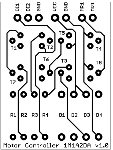
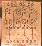
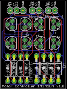
So our board has been designed, now we’ll need to print it out. Before printing, we firstly need to only print the layers we need and print in monochrome. In Eagle, click on the layers button (below the i) and select None. Now only select the top layer, the pads/vias, dimension and bPlace. I’ve put all my text on bPlace so that’s why I have it selected, don’t select tPlace because this has a border for each component which will definitely cause you problems as they’ll all be in copper. Now make the background white by going to Options -> User Interface, then in Layout select the Background as White. You should have something similar to the below.
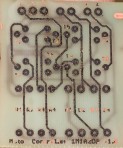
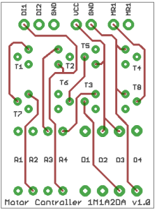
Now we need to save the image, most printers can do 600dpi so when saving the image it asks how much dpi we want to save it at, use 600dpi. In Eagle, we click File -> Export -> Image, select Monochrome, change the Resolution to 600dpi and save your file. You’ll see the image below.
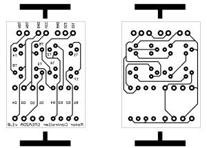
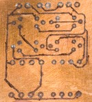
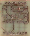
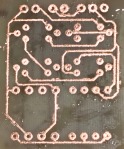
Lets do this for the bottom layer, this time we just want to show the bottom layer, the pads/vias, dimensions and nothing else. Our final step is to actually use a picture editing program to flip the top image horizontally so this is how everything looks now, imagine the PCB going in the middle of these images, so you sandwich them together on the PCB and they line up well.
You’re probably wondering what those dark black T’s are for? They are so you can align both layers to your PCB.
Cutting your PCB from the copper clad
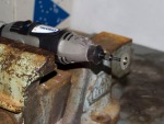
Now it’s time for us to cut our PCB out from the copper clad board we have. Measure it out with a ruler, mark the lines with pencil and then you can get out your dremel and start cutting.
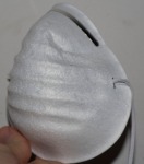
You want to position the dremel somewhere stable, I used a vice stand that was lying around. Grab your dust mask as this stuff is toxic, grab your metal diamond tipped cutting blade and make sure it’s all secure then let the cutting commence!
Edit: 21 December 2010 – I’ve found out that you can actually use tin snips to cut the board much more easily with less mess, I recommend it over the dremel. I purchased Aviation Tin Snips from Ebay for $8.
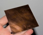
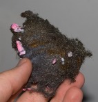
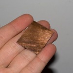
Once you’re done, you need to clean up the board. I firstly used Brasso to make the copper all shiny, use tissues or a soft cloth and keep wiping the board in a circular motion until it’s shiny. It’s okay if it turns the copper board black, just keep wiping the board and it’ll go away. If you don’t have Brasso you can just use Isopropyl alcohol with the rough side of a sponge to clean it and then dry with kitchen paper. Another way is to use steel wool and gently wipe the board in a circular motion.
It’s a bit hard to see but the copper board is much shinier.
Then use Isopropyl alcohol to finish it up (I didn’t have the pure kind so I used Isocol however it does have other ingredients in the mix so it’s not ideal).
Transferring the PCB design
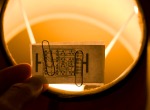
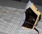
So print out your PCB design, cut them out and align them together by using a lamp and paper clips to help stabilise it.
Now use sticky tape to tape the sides that have the T shapes, this is so the iron gets the best contact to the paper achievable. Then slide in your PCB.
Grab the iron, turn it on maximum heat, make sure there is no water in it and press it onto the PCB for about 20 seconds and then slowly start moving the iron around the board, also go over the board using the tip of the iron. Remember to do the back side of the PCB too! Be sure to not burn the paper, you’ll see it change colour to light yellow a little so keep an eye that it doesn’t go past that. With my iron I left the protective cover on it, this helps it from sticking when moving over the board however it does mean that you’ll have to spend about 2 minutes on each side of the board but it really depends on the iron you have.
After you’ve finished ironing the board, give it a minute or two to cool down and then place it in some luke warm water for approximately 15 minutes. Once that’s done, gently start rubbing the paper on the PCB and you should begin to see the tracks. You can then slowly peel off the paper from the PCB and gently rub the PCB if some paper is left over. What I’ve found is that quite a bit of paper was really stuck on to the PCB and if you took a sponge or wet towel to it, it would actually start removing a tiny bit of toner.
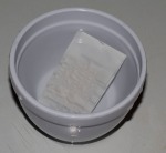
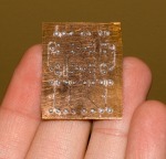
Maybe this means the toner wasn’t stuck on the board properly maybe this is where my main problem lied where sometimes I would see very small breaks in the lines so what I had to do is use a permanent marker with a super fine tip (0.4mm) and very carefully go over a few tracks, then because the tip was too large I wiped it a few times with a wet towel, eventually I was left with the board below.
Etching the PCB
This can be one of the most complicated parts of the PCB development process, please refer to my notes at the bottom for more information. Now you want to do this outside, grab the Hydrochloric acid, Hydrogen Peroxide, the glass container and smaller plastic containers.
Pour in the hydrogen peroxide to the small plastic container then transfer that to the glass container twice, then do the same with the hydrochloric acid but only once. The ratio is 2:1 (2 parts hydrogen peroxide and 1 parts hydrochloric acid). You want to pour the hydrochloric acid in slowly, you might see bubbling and it’s normal for the glass container to become a little hot. Once you are done, it can be a clear solution or it might be a bit yellow like mine is.
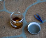
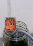
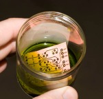
I’ve made a smaller solution of this in one of my smaller glass containers so we can see it working. Now you are ready to etch, have a small plastic container with water handy. I used a fish tank air pump to make some bubbles to keep the solution moving around and to also help the solution etch the board (explain in the Notes about Etching section).
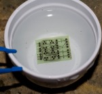
Using plastic tweezers, drop in your PCB into this solution and begin giving it a little swirl, in the next 30-60 seconds you might see it begin to dissolve some of the copper. Keep swirling and give it a few more minutes, after a while you’ll see the PCB turning pinkish and then light green, this is good. Once all the copper is gone, remove the PCB with your tweezers and drop it in some water to stop the etching. It took my PCB about 40-50 minutes to etch so keep a good eye on it. For better etching performance you want to suspend your board in such a way that it’s in the middle of the solution and not on the ground of the container.
Drop the PCB in your container with water, give it a few seconds and then remove the PCB, soak under a tap and dry it off. As you can see I’ve left this board in a bit too long, some of the text on my board is missing, I believe it’s due to the fact that I was cutting my boards too close to the corners, so I think you have to add on say 1cm to the edges of the board to give a better change of keeping your text.
Now we can remove the toner from the PCB, you can use a sponge, acetone or steel wool. If you use the sponge by itself you might find it’s hard to do if your toner is really suck on (which it should be) so I went ahead and used the steel wool which helped out quite well. The steel wool I used once mixed with water didn’t mix too well, eventually the steel wool will fall apart and begin rusting, so keep that in mind.
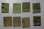
Be sure to take your time until you find something that works for you, it took me a few weeks to do this and a few failed boards as below. You can see the first few attempts the lines were too thin, the next few they were larger but if you look closely there are a few breaks in the lines, then I tested marking the boards with a permanent marker a few times.
Our board is ready for some drilling.
Drilling the PCB
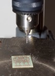
Remember to use your dust mask for this. Grab your drill bits, the two I needed were the 0.7mm for the resistors and transistors plus the 0.9mm for the diodes. Now it’s just a matter of time and patience to drill through the hole, believe me it does take some time so practice before hand (possibly on your failed PCBs). What I do is use a light close to the drill bit, then lower the drill almost until it touches the PCB and then slowly move it down until it makes an impression and then I can either drill the hole or lift it up and move it slightly. Now just repeat and we’re done.
Don’t expect it to be perfect, mine sure wasn’t but it was close enough.
Soldering the PCB
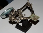
I was a bit rusty with my soldering iron but I just practiced on my failed boards with random components I’ve collected. I used a little holding mechanism and used the magnifying glass for support. Firstly we need to make sure that all our contacts are clean, wipe the board down with some Isopropyl alcohol.
My soldering technique is to apply the tip of the iron with some solder, wet that with a tissue, place it on the component to solder making sure I’m touching the pin and the copper contact and then slowly adding little bit of solder wire each time making sure to add the wire on the side opposite to the solder.
Now before getting carried away with soldering all components, it’s important to remember that this is a double sided board so it means we need to solder both sides of the PCB. So solder in components that are fairly spaced apart so that once you are done with the bottom side of them you can move on the soldering the top side. This is something that I would have missed; it turns out that manufactured PCB boards actually have copper through the holes drill in, this is called Plated-Through-Hole (PTH) where they use copper electroplating. The way hobbyists get around this is by using via’s but no need to that that for our PCB.
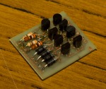
Once you’re done soldering, put on some more Isopropyl alcohol and use a little brush to wipe around the component contacts and that’s it we’re done. Now just closely inspect your contacts and just a little test with a 12V battery and some 12V fans, all working good! 😀
Final Thoughts
- Take you time going through the design process and leave more than enough space between components. On my PCB the transistors and resistors are too close along with the lines.
- Put similar components together. I should have switched the 39K and 390K resistors, so that it’s a bit neater; instead of being 39K, 390K, 39K, 390K it will be 39K, 39K, 390K, 390K. I had to unsolder 2 resistors because of this. Also buy some solder wick so removing components is easier.
- Use thin solder wire, sometime like 0.4 or 0.5mm, 0.8mm or higher makes it harder to solder components that are close to each other.
- Don’t expect your PCB to be similar quality to ones made at a PCB manufacturing plant.
- This process worked for me but may not work exactly for you, so try a variation of what worked for me or check what others have done.
- Keep trying and don’t give up.
Notes about Etching
I’ve leaned a few things from the etching process. This is how my etching first looked like:
Which is fine however it’s not fast enough, it’s important to use more than you think is necessary to etch the board, if you are only using just enough Hydrochloric acid & Hydrogen Peroxide to cover the board, it’ll take a long time so make sure you use quite a bit more.
The next thing is to not think something is wrong when your solution is light yellow, is just means you haven’t formed cupric chloride which is the final solution which eats the copper away. I say final solution because the Hydrochloric acid & Hydrogen Peroxide mixed together will oxidise and remove the starting amount copper you have. You need to add copper to the solution, so add only very thin pieces of copper or start your etching process. Adding long pieces of copper will work but slowly and if you add too much then you’ll have a dark black solution. If you want to learn more I highly recommend checking out the Etchant process links I provided at the top.
When you do have a dark black solution you add bubbles (air) or hydrogen peroxide to make it light green again. This light green means it’s ready for etching again and it make take an hour or more to “re-green” it.
If your etching is slow, you should add a bit more acid to help speed things up, careful not to over do it. If the etching is slow, it means that eventually the solution will penetrate the toner and will eat away the copper from your lines/pads.
Now the other way to etch is to actually pour in the Hydrochloric acid to a glass container, drop in some copper and then bubble it away. The oxygen from the air will oxidise the copper and then you’ll have cupric chloride, though this method takes a while to do. Another way to quicken it up is to grab your copper, put it over a stove or a fire until it goes bright red (means it’s oxidising), then drop it in your Hydrochloric acid and you’ll have cupric chloride.
 ,
,