It’s been 5 years since I started making GBCartRead (GB Cart Shield) using the Arduino to read Gameboy ROMs and save games. GB Cart Slots at the time of this post are becoming harder to find (Aliexpress are selling used ones) plus I have some time on my hands so I think it’s time to re-do it without the need of the Arduino. There have been a few users ask if GB Cart Shield supported the Gameboy Advance which it doesn’t, so I will look into supporting that for this new project which I might call – GBxCartRead (the x shows it supports GB/GBC/GBA).
I’d like to remove the shift registers that the GB Cart Shield currently has and look for an AVR MCU which has enough pins to cover the GB slot pins at a reasonable cost. There are few options like the ATmega162, 165, 169.
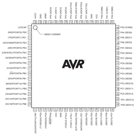
I choose the ATmega169A for $6 as it came with free shipping from RS and I will be using it for another project, it’s pretty big. It has 54 I/O lines, way more than what we need though it will allow us to use 3 complete PORTs dedicated to the GB I/O.
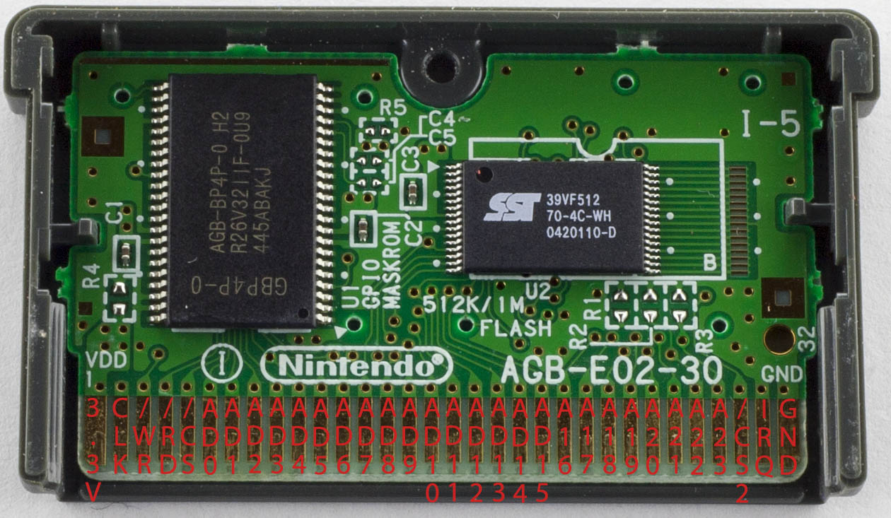
GBA cartridges are similar to GB carts except that they require 3.3V, use 3.3V logic, have 24 address lines and they switch the first 16 address lines into data lines when reading the ROM. As per the GB carts, you pulse WR low to write, RD low to read and CS low whilst doing either. They have a CS2 line which is dedicated to the SRAM, pulse CS2 low to access it. An upside over GB carts is that we don’t have to do any bank switching for reading the ROM due to the 24 bit address line (32Mbit max) but a downside is that the GBA cart header doesn’t contain any useful information about ROM size, RAM size, etc. There is however a useful gba.xml file from the MAME project (\mame\hash in the source) in which they have documented which cartridges contain what chips.
At first SRAM/FRAM was used, then they started using Flash for save games which works the same way as SRAM for reading but writing is different and some carts have an EEPROM which are accessed serially. There are 2 different Flash chips we need to account for (as they have different writing methods) with 512Kbit/1Mbit sizes, 2 different sizes of EEPROM (4Kbit/64Kbit) and 2 different SRAM sizes (256Kbit/512Kbit). This is beginning to become more complicated than I first thought but I’ll continue on.
In order to accommodate both the GB and GBA we will need a switch to change the ATmega input voltage from 3.3V to 5V and for the USB interface to the PC, the are a few options we could go with:
- Use a USB to serial converter like an FTDI. This might be the fastest solution in terms of USB bandwidth throughput. I checked out pricing for these and other brands however the cheapest ones available on Element14 are $3 each. There was an article from Hackaday about the alternative CH340G which are 41c from Ebay, hopefully they work, I have some on order for testing.
- Use V-USB directly on the ATmega but this won’t work under 3.3V as the ATmega169A only supports a max clock speed of 10MHz, sure we could overclock it but I’d rather not do that. The ATmega169 non-A/PA version can go to 12MHz or I could use the ATmega162 which also can.
- Use V-USB on an ATtiny and use that to communicate with the ATmega via SPI, we could use a 74AHC125 logic buffer to step down 5V to 3.3V. This is the option I’ve gone with for the moment, it makes things more complex but it’s all I have until the serial converter chip arrives (I could use an external usb to serial converter that I have, if I knew it the CH340G would work well but for the sake of it, lets try something different as a proof of concept that this other way works too)
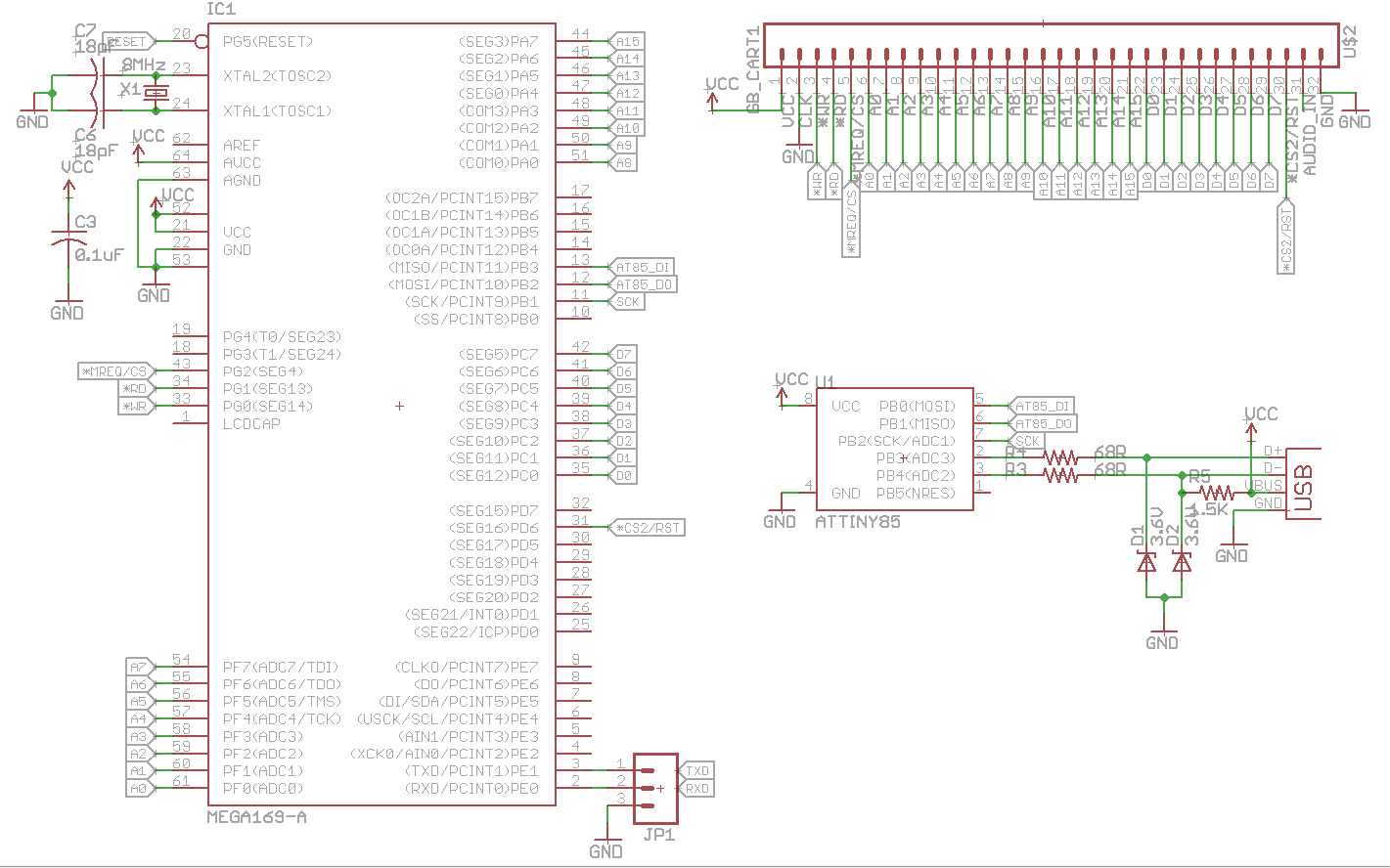
For this part I can re-use some of my code from GBCartRead, makethe ATtiny85 “USB to SPI bridge” you could call it (ATtiny will be master) and make sure the Gameboy cartridges works so it’ll all be at 5V for the moment so no need for the logic buffer yet. Since we’ll have a bridge between the ATtiny and ATmega, I need to make the ATmega have a very simple interface so that all the processing is done on the PC and the ATtiny will just pass on our command and data to the ATmega. Data will be transferred in 64 byte chunks.
#define USB_SET_START_ADDRESS 'A'
#define USB_SET_END_ADDRESS 'E'
#define USB_READ_ROM_RAM 'R'
#define USB_WRITE_RAM 'W'
#define USB_SET_BANK 'B'
#define USB_RESET_LOOP 'L'
#define USB_TEST 'T'
...

// Enable SPI
DDRB |= (1<<PB3); // MISO
SPCR = (1<<SPE);

while(1) {
	rd_wr_csmreq_cs2_reset();
	while (!(SPSR & (1<<SPIF))); // Wait for data
 	receivedChar = SPDR;
We firstly have our commands, 1 character long to keep things short, enable SPI, reset our common lines like RD, WR, etc and then await for commands/data from the ATtiny.
// ATtiny side
// 'A' - Send and store the start address
else if (replyBuf[0] == USB_SET_START_ADDRESS) {
	spi_transfer(replyBuf[0]); // Pass on command

	// Send address
	uint8_t x = 1;
	while (replyBuf[x] != 0) {
		spi_transfer(replyBuf[x]);
		x++;
	}
	spi_transfer(0);

	// Store current address (skip the first char)
	currentAddress = strtol((char*) &replyBuf[1], NULL, 16);
}
...

// ATmega side
void spi_read_chars(void) {
	uint8_t x = 0;
	while (1) {
		while (!(SPSR & (1<<SPIF)));
		receivedBuffer[x] = SPDR;
		if (receivedBuffer[x] == 0) {
			break;
		}
		x++;
	}
}
...

if (receivedChar == 'A') { // Set address in variable
	spi_read_chars(); // Read start address
	address = strtol(receivedBuffer, NULL, 16); // Convert address string in hex to dec
}
One example of a command is settings the start address which is useful for reading the ROM, reading RAM and writing to the RAM. The ATtiny would send the ‘A’ for address and a hex value for the address with a terminate string byte (0). The ATmega would receive the ‘A’ command and read the rest of the string until 0 is reached and then convert that string containing the hex number into a decimal number, I used hex as it uses less characters to send than decimal. The rest of the communication between the ATmega / ATtiny is more or less like this, it did take a while to get everything working just right (I used the USART port to debug).
// Read ROM/RAM from address (and increment) until anything but 1 is received
else if (receivedChar == 'R') {
	receivedChar = 1;
	while (receivedChar == 1) {
		SPDR = read_8bit_data(address);
		while (!(SPSR & (1<<SPIF)));
		receivedChar = SPDR;
		address++;
	}
}
...

// Set the address and read a byte from the 8 bit data line
uint8_t read_8bit_data(uint16_t address) {
    set_16bit_address(address);

    cs_mreqPin_low;
    rdPin_low;
    asm volatile("nop"); // Delay a little (minimum needed is 1 nops)
    uint8_t data = PIN_DATA7_0; // Read data

    rdPin_high;
    cs_mreqPin_high;

    return data;
}
Let’s have a look at reading the ROM from the ATmega side. We wait for the ‘R’ read ROM command to be received and then we use the start address that we had stored before to read the data which we load into the SPI data register. When an SPI transfer comes in, it sends the data we read before, we check that the received command is still 1 and then increment address (the ATTiny side holds the end address so it knows when to stop reading from our PC program). The actual reading data function is much like the same as the original GBCartRead program.
void write_8bit_data(uint16_t address, uint8_t data, uint8_t type) {
	...
	// Pulse WR and mREQ if the type matches
	wrPin_low;
	if (type == MEMORY_WRITE) {
		cs_mreqPin_low;
	}
	...

else if (receivedChar == 'B') {
	spi_read_chars(); // Read start address
	uint16_t bankaddress = strtol(receivedBuffer, NULL, 16); // Convert address string in hex to dec

	while (!(SPSR & (1<<SPIF))); // Wait for bank write data
	receivedChar = SPDR;

	if (receivedChar == 'B') {
		spi_read_chars(); // Read data
		uint8_t data = atoi(receivedBuffer); // Convert data string to dec
		write_8bit_data(bankaddress, data, BANK_WRITE);
	}
}
Apart from that, I have combined bank switching and RAM writing together just by toggling a type byte. Speaking of bank switching, we firstly receive ‘B’ command then the bank address in hex, the ‘B’ command again and the data in decimal as it shouldn’t be more than 1 byte.
All that’s left now is to modify the original C program to work with V-USB and make a few changes in what it does (like setting the start address, end address and transferring that over) but ~70% of it is mostly the same.
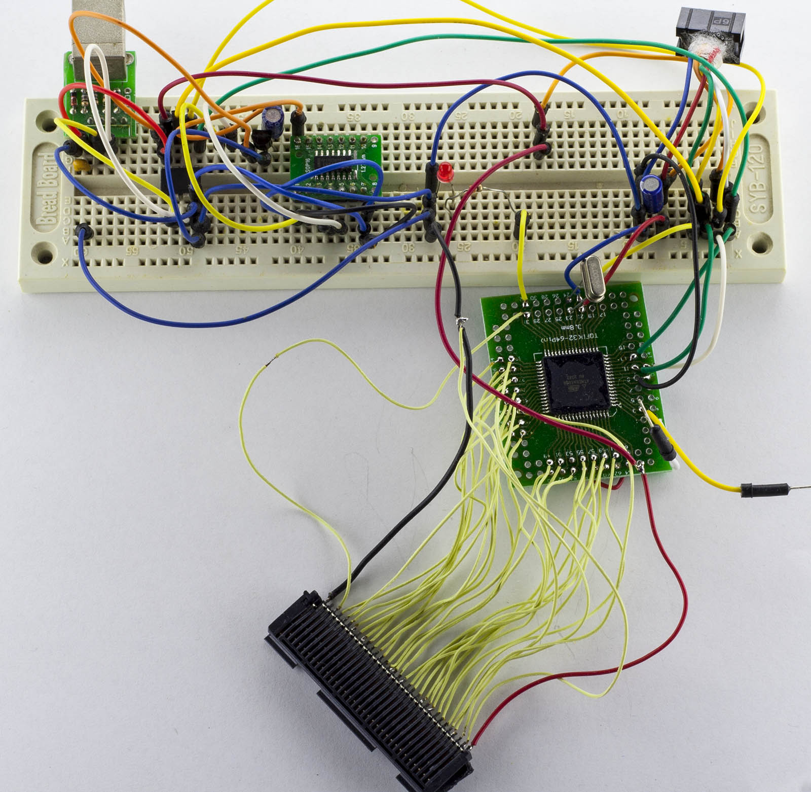
(ignore the logic buffer, just there for testing)
After lots of testing, I can confirm that reading ROM, reading RAM and writing RAM to Gameboy cartridges works well, the speed is 128KB in 12 seconds so it isn’t as fast as the original GBCartRead but once I move over to the USB to serial solution and if it works well, we should be able to match the GBCartRead Arduino speed of 400K baud or go higher (at 8MHz with the ATmega it says it can do 1M baud).
Download GBxCartRead v0.1
GBxCartRead – Part 1: Design and Testing Gameboy Carts
GBxCartRead – Part 2: Switching to CH340G, GBA ROM reading, SRAM read/write and determining sizes
GBxCartRead – Part 3: GBA EEPROM Read/Write & Flash Write and Determining Sizes
GBxCart RW v1.0 Released


Why don’t you use Arduino Mega board? It has a lot of I/O pin and it’s easy to use even for beginners. On aliexpress a chinese mega go for $7 and it has all you need.
Very good project, I will follow you.
Hi Roxas,
Yep the Arduino Mega would suit for the GB/GBC carts but not for the GBA carts that require 3.3V unless you did some mods to it.
Also I like to build things mostly from the ground up when I can 🙂
I see, you are great. But in this way I don’t think that a lot of people like me can make this project :'(
By the way i will follow this project, it’s very interesting. I hope that i can do it myself, but I don’t think so.
Hi! I’m looking for something like this working with Arduino(GBA cards), like you said. Have you ever found something? Thank you!
Hi there,
you wrote about a successor for the GBC Shield. Will it be this device?
Would be great to read GBC and GBA saves 😉
greets,
Ralf
Hi Ralf,
Yep that’s correct, this will read GB/GBC/GBA saves.
Hi, i wanna know if i can reproduce it with just an arduino mega 2560 pro mini, and if this possible, i need something of resistors about USB?
Greets, Kuro.
I mean if i use a switch for select 3v3 or 5v
It might be possible, you just have to make sure the ATmega2560 will run at 8MHz so it will function correctly at 3.3V too. Another way is to use level shifters to convert 5V to 3.3V for GBA carts on all the lines going to the cartridge.
Yep, i watched some people who got their mega 2560 at 8MHz.
I will test it and if it works i say to you cause i want to have backups of my fav games and never lose it.