From our last part we were able to read the data from the SRAM using an ATmega but found that we couldn’t run the SRAM with a 100MHz clock and when reading the data out it was noisy/inaccurate – even re-reading the same address ranges would give different results. In this part, I’ve made some prototype boards and we’ll look into fixing the reading issues.
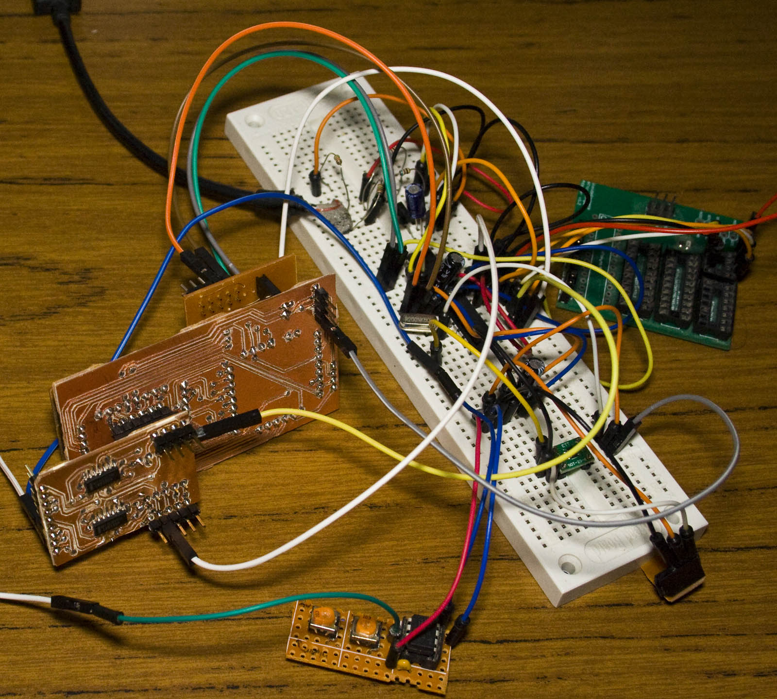
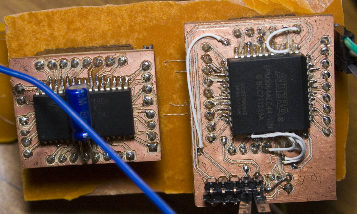
I decided to make a new board for the CPLD so I could mount it and the SRAM to a main board and also made a buffer logic board to be mounted under the main board plus there is also a very small board for the 50MHz oscillator.
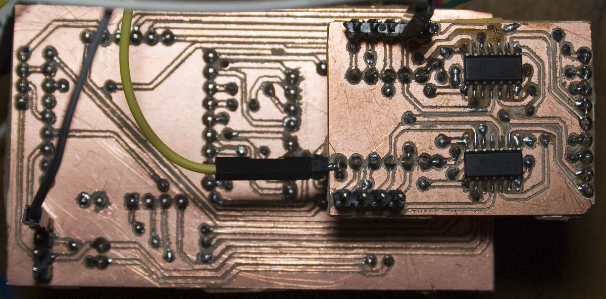
For the buffer board, I’m using 2x 74LVC125 each one does 4 inputs. What I didn’t realise is that these are active low so I’ve modified my CPLD code to suit: CPLD_LogicAnalyser_v0.2
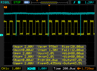
Upon testing all the boards together it seems to be working however now I saw some jitter when reading the same address range (start address shown by the blue line)
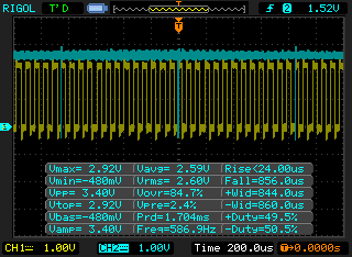
I decided to enable the clock output on the ATmega and use that for writing and reading – it worked perfectly. I tried running the 50MHz clock when writing and 20MHz clock when reading and it also worked well, so the 50MHz for reading must be a bit too fast for the SRAM. I tried using an SN74LVC1G3157 analog switch to switch between the two clocks and it worked well.
Here’s all the schematics/boards (CPLD_LogicAnalyser_v0.2_Schematic-PCBs) and ATmega code (CPLD_LogicAnalyser_v0.2_Rev2).
------------- 65 times, 0.769231 mhz
------------- 97 times, 0.515464 mhz
------------- 96 times, 0.520833 mhz
------------- 96 times, 0.520833 mhz
------------- 96 times, 0.520833 mhz
------------- 96 times, 0.520833 mhz
------------- 96 times, 0.520833 mhz
------------- 96 times, 0.520833 mhz
------------- 97 times, 0.515464 mhz
------------- 96 times, 0.520833 mhz
------------- 96 times, 0.520833 mhz
------------- 96 times, 0.520833 mhz
------------- 96 times, 0.520833 mhz
------------- 96 times, 0.520833 mhz
------------- 96 times, 0.520833 mhz
------------- 97 times, 0.515464 mhz
The first reading can be ignored as we just triggered anywhere on the signal but the rest of the readings are pretty spot on, only a difference of 1 value in all the readings.
------------- 4 times, 12.500000 mhz
------------- 11 times, 4.545455 mhz
------------- 11 times, 4.545455 mhz
------------- 11 times, 4.545455 mhz
------------- 11 times, 4.545455 mhz
------------- 12 times, 4.166667 mhz
------------- 11 times, 4.545455 mhz
------------- 11 times, 4.545455 mhz
------------- 11 times, 4.545455 mhz
------------- 11 times, 4.545455 mhz
Increasing the input clock and still looking good. Now all that’s left to do is give it a real test which uses all the inputs and implement the ATmega output clock for slower capture rates using the timer before committing to this design.
Building a CPLD Based Logic Analyser – Part 1: SPI writing in Verilog, Testing the basics and modifying Scanalogic SCL files to insert our own data
Building a CPLD Based Logic Analyser – Part 2: Switching to the EPM3064 CPLD
Building a CPLD Based Logic Analyser – Part 3: Testing the Cypress 1Mbit SRAM
Building a CPLD Based Logic Analyser – Part 4: Reading data/triggering with an ATmega with V-USB and testing
Building a CPLD Based Logic Analyser – Part 5: Prototype boards and fixing reading issues
Building a CPLD Based Logic Analyser – Part 6: Software side, trigger/sampling options, hardware changes and possible changes for a 100MHz analyser
Building a CPLD Based Logic Analyser – Part 7: PCBs arrived, move to Sigrok Pulseview, simple GUI program and a few software modifications


