From our last part we added trigger options/sample rates, made small hardware changes and came up with possible design changes which could give us an 100MHz logic analyser. It’s been 6 months since my last update – I’ve just been working on little improvements and have enough that I can report on them all now. In this part we’ll take a look at our PCBs, move from MiniLA to Sigok Pulseview, a simple GUI interface and a few software modifications.
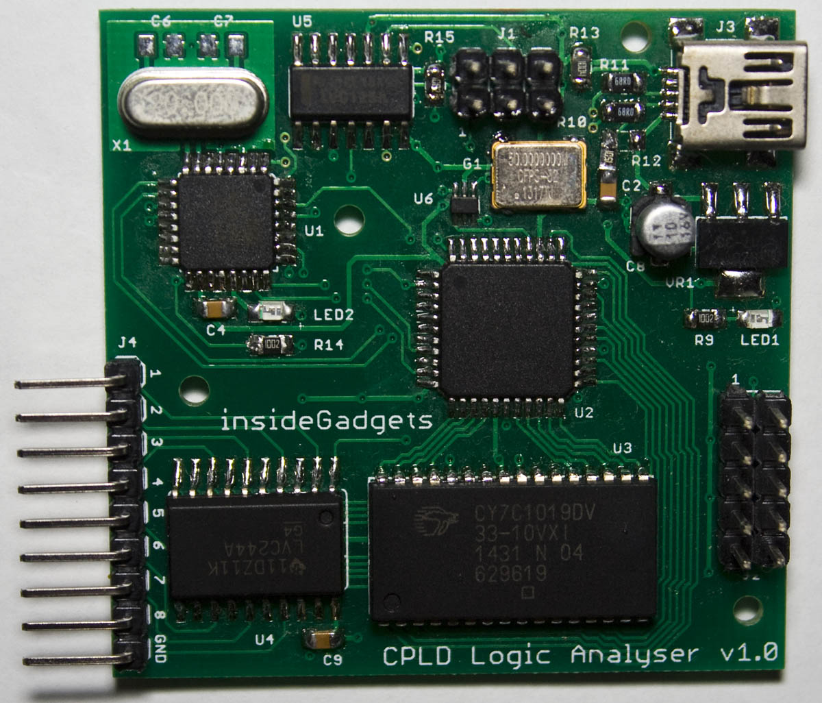
First things first, the PCBs arrived so I built one up quickly, the SRAM was a little tricky to solder and I reflow soldered the oscillator and Mini USB connector (I seem to always have issues with the pins bridging on the Mini USB when using an iron). Both the ATmega and CPLD were programmed successfully however the logic analyser just didn’t work properly. The CPLD was getting quite hot and turns out that some pins were stuck at VCC or GND no matter what I did and 1 pin on the ATmega also had an issue.
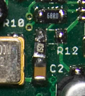
I found that the 1.5K resistor used for the USB was connected to 5V instead of the 3.3V regulator so potentially this could have caused the issue, good thing a cap with 3.3V was close by so I soldered it to that. I replaced the CPLD and jumper wired another pin on the ATmega to it and everything worked this time around. Just to be sure that everything was really ok, I built up a second PCB and confirmed it all worked.
I tested the logic analyser on a Gameboy cartridge and found that even when using 100K resistors, you could see a pretty bad load that its applied. I increased the resistors to 1M and then I settled with 4.7M.
Faster USB transfer
Previously I was using 2 bytes when transferring the 8 bits worth of data, the main reason being that I wasn’t able to use “0” as an actual result as it would mark the end of the string.
uint32_t samples_size[7] = {8128, 16002, 32004, 64008, 96012, 131064};
...
if (rq->bRequest == USB_TRANSFER && addressCount < addressEnd) { // custom command is in the bRequest field
	nextDigit = &replyBuf[-1];

	// Loop 254 times to send this data over USB
	PORTB |= (1<<captureLED); // Show activity
	for (uint8_t a = 0; a < 254; a++) {
		PORTB |= (1<<nextaddressPin); // Tell the CPLD we want the next address
		asm ("nop"); // Wait a little bit for CPLD/SRAM to show proper reading
		asm ("nop");
		asm ("nop");

		// Read and combine PD7, PB0 & PC6-0
		uint8_t reading = (PIND & 0x80) | ((PINB & 0x01) << 6) | (PINC & 0x30) | (PINC & 0x0F);
		*++nextDigit = reading;

		PORTB &= ~(1<<nextaddressPin);
		addressCount++;
	}
	PORTB &= ~(1<<captureLED);

	usbMsgPtr = replyBuf;
	return sizeof(replyBuf);
}
After taking another look at this, I figured that if I came up with sample depths in multiples of 254 that I no longer need an ‘x’ to indicate the end of the transfer, instead now we just don’t send anything back if all data has been read out. Before it used to take 40 seconds to transfer the full 131Kbit and now it’s down to 20 seconds.
Changing from MiniLA to Sigrok Pulseview
Initially I had the logic analyser’s output file work with MiniLA and it was working nicely however it didn’t have all the protocol decoding that Sigrok Pulseview did so I tried re-downloading Pulseview and this time on my Windows XP machine it loaded up fine (a previous version didn’t load which is why I went with MiniLA).
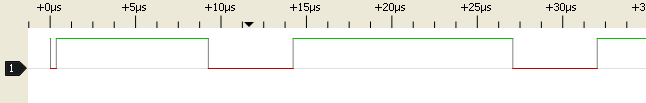
After a look around of their example files, they have 3 files which they zip up:
![]()
The logic-1 file contains the data – in our example 06 (110 in binary) would be a high on the 2-3 pins and 0E would be high on pin 2-4 (1110 binary) which is easy to set our data format to suit.
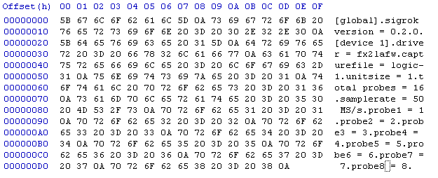
The metadata file contains the sample rate and mapping of the probes, the only thing we need to change is the sample rate.
// Create the PulseView metafile
char metadata_p1[] = {0x5B, 0x67, 0x6C, 0x6F, ...
char metadata_p2[] = {0x0A, 0x70, 0x72, 0x6F, ...

FILE *metaFile = fopen("metadata", "wb");
if (metaFile == NULL) {
	fputs ("File error",stderr);
	exit (1);
}
fwrite(metadata_p1, 1, strlen(metadata_p1), metaFile);
fwrite(sample_rate_text[sample_rate], 1, strlen(sample_rate_text[sample_rate]), metaFile);
fwrite(metadata_p2, 1, strlen(metadata_p2), metaFile);
fclose(metaFile);
In our C reader program we store the first half of the file leading to the sample rate, then insert the sample rate and then add in the second half of the file. The version file is just a 1 byte file which remains static.
7za.exe a -tzip %s.sr logic-1 metadata version
Once we have all 3 files, we can use the command line of 7zip to zip it all up and have it ready to open with PulseView.
Simple GUI program and a name
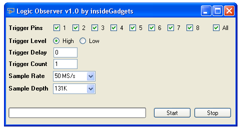
I decided that I needed a name other than “CPLD Based Logic Analyser” so after searching for similar words which are more unique, I went with Logic Observer.
The command line interface works good but I wanted to use something easier to control the logic analyser with so I developed a simple GUI program using Microsoft Visual C# 2010 Express. Personally I’ve never used Visual C# before (I’ve used Visual Basic only once or twice about 8 years ago) but the drag and drop functionality makes things easy.
After playing around with the code and finding some examples, what I’m doing is just the front end in Visual C# and it’s just hiding the calls to the command line interface, this way I could keep both programs up to date easily and I added arguments to the command line program to facilitate this. The progress bar was part that took the longest to get right – I’m using one thread to read the size of a “progress.txt” file, each byte represents 1%.
Adding check/cancel ability when waiting for trigger
One problem I had was when you are waiting for a trigger, there was no real way to check the status/cancel unless you unplug/reconnect the logic analyser.
At first I tried running usbPoll constantly when waiting for a trigger however as you see it would take up valuable time so checking on the pins for a trigger could take slightly longer. After adding a timer for 26ms and then polling the usb, it looks better now.
I use another thread on the GUI to check on the status of the logic analyser to see if we’re waiting for a trigger, if not then we read out the data. Once the cancel button is pressed, we open up another command window to execute the /cancel command.
Correcting trigger timing and pin reading speed
for (int8_t x = 1; x < 10000; x++) {
	PORTB |= (1<<PB0);
	_delay_loop_2(x);
	PORTB &= ~(1<<PB0);
}
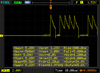
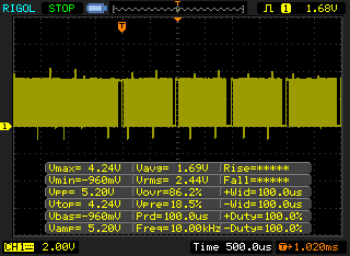
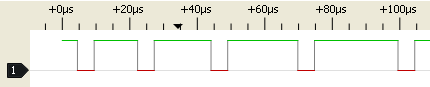
It was now time to test when triggered how much data would actually show up on the logic analyser as it could take a few uS before any data was being recorded by it. The way I did this test was to have a pulse which would increase in its delay time every loop.
I’ve always been setting the CPLD address equal to 50 cycles before the trigger point which works fine for under 10MHz however for 50MHz it’s not far back enough.
After a bit more testing, going to 350 cycles is just enough to capture the start of the first pulse which equates to about 7uS of delay which is a little bit more than I would have expected.
uint8_t pin_reading = (((PIND & 0x80) | ((PINB & 0x01) << 6) | (PINC & 0x3F));
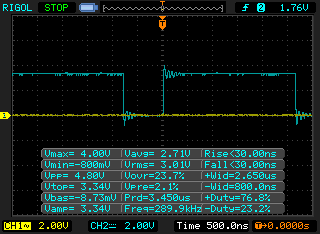
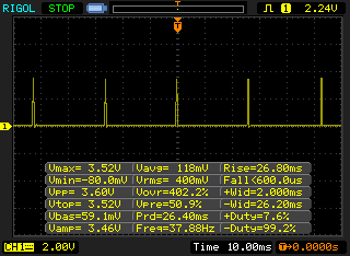
Upon further investigation it seems that reading the pins, aligning them to fill in all 8 bits and checking for the trigger high/low conditions takes about 2.6uS.
uint8_t pinb_reading = ((PINB & 0x01) << 6);
uint8_t pin_reading = ((PIND & 0x80) | (PINC & 0x3F)) | pinb_reading;
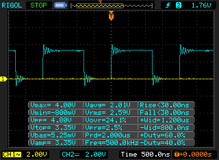
After a little bit of testing, we can reduce this by half by placing the PINB read and shift in it’s own line and now I can reduce the cycles we capture before the trigger down to 290 while keeping about 50-500nS for the pre-trigger. For the next version I might try to see if I can switch bit 6 with another pin so I don’t have to bit shift. I’ve also added a pin change interrupt for all the trigger pins so we can trigger just that little bit more quickly.
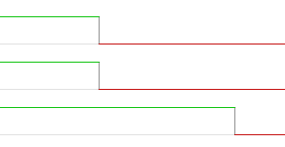
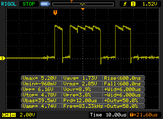
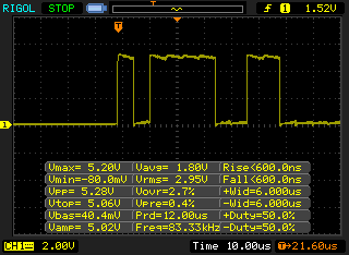
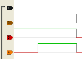
When testing the triggering I noticed that the skew rate of pin 8 is 1 clock cycle behind the rest of them which is a little odd as it’s length compared to the first pin is 7mm shorter.
PORTB |= (1<<nextaddressPin); // Tell the CPLD we want the next address
asm ("nop"); // Wait a little bit for SRAM to show proper reading
asm ("nop");
asm ("nop");

// Read and combine PD7, PB0 & PC6-0
uint8_t pinb_reading = ((PINB & 0x01) << 6);
uint8_t reading = ((PIND & 0x80) | (PINC & 0x3F)) | pinb_reading;
*++nextDigit = reading;
PORTB &= ~(1<<nextaddressPin);
I thought the issue could be the reading of the SRAM so I tried adding more 2 more nops and the problem went away (I could also remove all nops but it gave me a false reading of high right at the start but the rest of the data seemed fine but I didn’t look too much into it).
Download Logic_Observer_v1.0_Dev (development version)
I think that covers everything I’ve wanted to change, in a few days we should have a new product ready for sale!
Edit: The Logic Observer is now available for purchase
Building a CPLD Based Logic Analyser – Part 1: SPI writing in Verilog, Testing the basics and modifying Scanalogic SCL files to insert our own data
Building a CPLD Based Logic Analyser – Part 2: Switching to the EPM3064 CPLD
Building a CPLD Based Logic Analyser – Part 3: Testing the Cypress 1Mbit SRAM
Building a CPLD Based Logic Analyser – Part 4: Reading data/triggering with an ATmega with V-USB and testing
Building a CPLD Based Logic Analyser – Part 5: Prototype boards and fixing reading issues
Building a CPLD Based Logic Analyser – Part 6: Software side, trigger/sampling options, hardware changes and possible changes for a 100MHz analyser
Building a CPLD Based Logic Analyser – Part 7: PCBs arrived, move to Sigrok Pulseview, simple GUI program and a few software modifications


