From our last part we switched to the EPM3064 CPLD for our logic analyser. In this part we’ll use the Cypress 1Mbit SRAM to store the data that we capture.
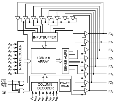
It’s a parallel SRAM which can run at 100MHz which allows us to save time compared to a regular 8 pin SRAM as we don’t have to clock in the address and clock in the data. All we have to do now is set the address pins, feed in the data and set the CE/WE pins low, the perfect job for a CPLD.
Writing and reading to the SRAM is fairly easy – to write we pull CE and WE low and to read we pull CE and WE low. In all other states the outputs are in high impendance, this allows us the option of adding more SRAM chips.
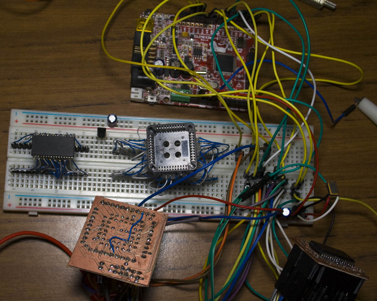
In order to test out the SRAM and the clock feed to the CPLD, I’ll have the CPLD increment an 8bit number which will be written to the SRAM and then read out with an MCU.
reg [5:0] readincrement;
output [16:0] address;
reg [16:0] address;
inout [7:0] data;
reg [7:0] data;
output ce;
wire ce;

always @ (posedge clockin) begin
	if (!reset) begin
		address <= 17'b0;
		data <= 8'bz;
		readincrement <= 1'b0;
	end
	else begin
		if (writing) begin
			address <= address + 17'b1;
			data <= data + 8'b1;
		end
		else begin
			data <= 8'bz;
			if (readincrement == 1 && readpulse) begin
				address <= address + 17'b1;
			end
			readincrement <= readincrement + 1'b1;
		end
	end
end

assign ce = (reset) ? clockin : 1'b1;
After using the pins for the address and data pins there aren’t many pins left. One will be our global clock, our reset pin, a writing pin which the MCU sets which will make the CPLD increment the address and data, a read pulse which the MCU sets high and low to increment the read address when reading the SRAM so the CPLD doesn’t keep advancing address locations as fast as it could.
The CE of the CPLD connects to the SRAM CE and is set high and low in line with the clock in as long as reset is high by using the assign method, this is the only way I’ve found with this type of CPLD in order to give a 1 to 1 clock ratio to cycle a pin high and low. By using the inout type for data, this allows us to change between an input, output or high-z – this is needed so that it doesn’t load down the SRAM when reading from it. For reading the SRAM data, I’m using an Olimex STM32 only because I don’t have anything else that runs with 3.3V.
Download cpld_sram_modelsim, cpld_sram_reading and cpld_sram_quartus.
Results file: cpld_sram_output
00000000
10000000
10000000
10000000
01000000
11000000
00100000
10100000
10100000
01100000
11100000
00010000
Here’s how it all looks and it seems to be working ok. The results seem to repeat the same number randomly which I think is because of how the read pulse is configured as there is a chance that it won’t move to the next address so I’ll need to work on a solution for that.
data <= 8'bz;
if (readpulse == 1 && readok == 0) begin
	readok <= 1'b1;
	address <= address + 17'b1;
end
if (readpulse == 0) begin
	readok <= 1'b0;
end
Edit: By adding another register it works good now. Download cpld_sram_quartus_v2
Once I test the actual reading of a frequency, I’ll have 8 data pins free on the CPLD so I can use these to control WE / OE pins and will need a buffer chip for the data. In the long run I would like to use SDRAM memory running at 133MHz+ however this CPLD variant doesn’t work that fast so perhaps I will use a Xilinx XC2C32A CPLD but I’ll leave that for version 2 of this project.
Building a CPLD Based Logic Analyser – Part 1: SPI writing in Verilog, Testing the basics and modifying Scanalogic SCL files to insert our own data
Building a CPLD Based Logic Analyser – Part 2: Switching to the EPM3064 CPLD
Building a CPLD Based Logic Analyser – Part 3: Testing the Cypress 1Mbit SRAM
Building a CPLD Based Logic Analyser – Part 4: Reading data/triggering with an ATmega with V-USB and testing
Building a CPLD Based Logic Analyser – Part 5: Prototype boards and fixing reading issues
Building a CPLD Based Logic Analyser – Part 6: Software side, trigger/sampling options, hardware changes and possible changes for a 100MHz analyser
Building a CPLD Based Logic Analyser – Part 7: PCBs arrived, move to Sigrok Pulseview, simple GUI program and a few software modificationsbit SRAM


