From our last part we looked at testing the idea with the EPM240 board, in this part we’ll switch over to the EPM3064 CPLD to move away from the development board.
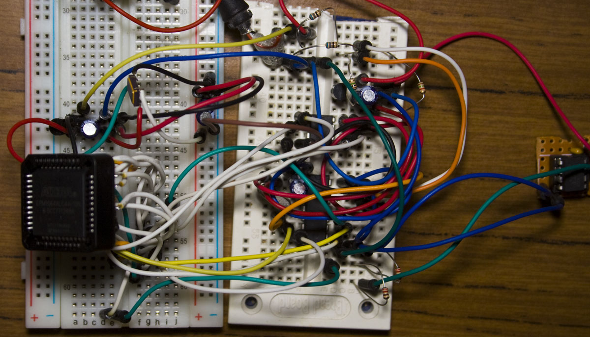
The Altera EPM3064ALC44-10N is a low cost 100MHz CPLD for $3 in a PLCC 44pin package with 64 LEs and 34 usable pins. The oscillator I’m using is 50MHz which I pulled from another board and all we need is to connect it to VCC, pull it’s enable pin high and that’s it. I was curious about how much current it consumed, it was about 13-15mA.
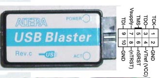
We can connect our USB Blaster to our CPLD by connecting up the 4 wires, TCK to TCK, TDI to TDI, TDO to TDO and TMS to TMS; as you can see you don’t connect them together like you do for the MISO of one device the MOSI of the other.
There is a 74HC125D buffer in the USB Blaster which isn’t powered by USB, it’s the VCC pin on the programmer cable and thus needs to be powered by the same voltage as the CPLD, I believe this is to allow compatibility with CPLDs running on different voltages.
Initially there was a problem where no data was being written to the SRAM even though the signals looked correct, I just had to connect the ground points between both devices a bit closer and that sorted it out.
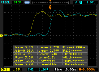
I was taking a look at the code again and we could potentially remove the CS line from the CPLD pass through but we shouldn’t do that for the SO line (SRAM to the ATtiny) because of the propagation delay from the the input of the CPLD to the output due to the sampling happening at 50MHz which from the above image looks to be about 25ns. The data would be out of sync to the CLK signal at higher speeds.
always @ (posedge CLKin)
begin
	if (!RESET) begin
		SI_OUT <= SI_IN;
		SO_OUT <= SO_IN;
		SCK_OUT <= SCK_IN;
	end
	else begin
		SCK_OUT <= ~SCK_OUT;

		OUT1 <= IN1;
		OUT2 <= IN2;
		OUT3 <= IN3;
		OUT4 <= IN4;
		SI_OUT <= IN1;
	end
end
After taking out all the unnecessary parts in my code, all it really has to do now is flip the clock on and off to bring us down to 25MHz and just feed the inputs to the outputs. When re-compiling this code it only takes up 7 LEs.
Technically the SRAM that I’m using should only support a maximum clock of 20MHz but running at 25MHz still seems to produce usable results. I have a Cypress 1Mbit SRAM 100MHz chip with an address width of 17 x 8 bits so for the next part I’ll see if I’m able to interface with it.
Building a CPLD Based Logic Analyser – Part 1: SPI writing in Verilog, Testing the basics and modifying Scanalogic SCL files to insert our own data
Building a CPLD Based Logic Analyser – Part 2: Switching to the EPM3064 CPLD
Building a CPLD Based Logic Analyser – Part 3: Testing the Cypress 1Mbit SRAM
Building a CPLD Based Logic Analyser – Part 4: Reading data/triggering with an ATmega with V-USB and testing
Building a CPLD Based Logic Analyser – Part 5: Prototype boards and fixing reading issues
Building a CPLD Based Logic Analyser – Part 6: Software side, trigger/sampling options, hardware changes and possible changes for a 100MHz analyser
Building a CPLD Based Logic Analyser – Part 7: PCBs arrived, move to Sigrok Pulseview, simple GUI program and a few software modifications


