From our last part we made some prototype boards including the buffer board and fixed the reading issues. In this part we’ll look at the software side to display the data we extract, add trigger options/sample rates, some hardware changes and possible design changes which could give us an 100MHz logic analyser.
Software for displaying our data
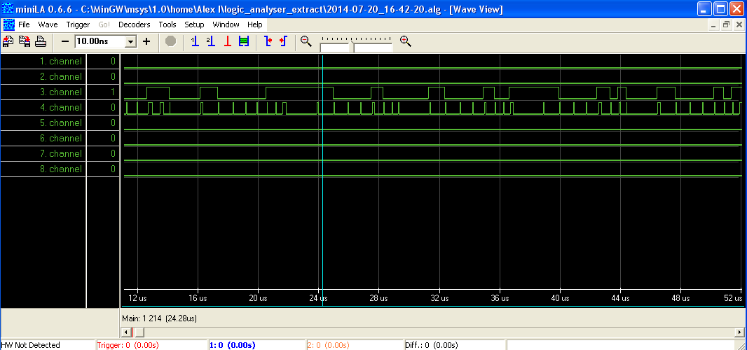
I had a look around at some software options that would just work out of the box and settled with one called MiniLA, they also had made an 100MHz logic analyser – it’s a beefier version of what I’m trying to achieve, their one has 32 channels and the CPLD/SRAM alone would cost $25-35 (about $40-50 in Australia) where as I’d like to make a small 8 channel one with USB (and it’s a learning experience for me too).
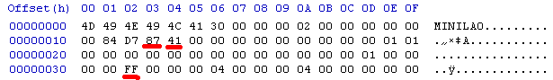
After looking around at the file format, it’s similar to how I was sending my data, so I was able to figure out how the data was formed – 00 00 FF 00 would set channel 1 to 8 all high for one time period. From the picture above, to change the time scale units from us to ns, you can change 41 to 42 and to change the time scale total length from say 2.52 to 2.62 ms you’d change 87 to 88. This should give us the flexibility to change time scale units depending on the clock we select.
Trigger/sample options
As the ATmega will act as the trigger source, I’ve been able to add options such as choosing which pin to trigger on, trigger level – high or low, trigger delay, trigger count – how many triggers we should wait for, sample rate and number of samples.
// Setup Timer 0 at 10MHz
DDRD |= (1<<PD6); // OCR0A as output
TCCR0A = (1<<COM0A0) | (1<<WGM01); // Toggle OC0A on Compare Match
OCR0A = 0;
TCCR0B = (1<<CS00); // No prescaler
...
// Change analog switch to 50MHz clock
if (settings[SAMPLE_RATE] == 0x50) {
	PORTD &= ~(1<<analogswitchPin);
}
else { // Or to AVR timer clock
	OCR0A = settings[SAMPLE_RATE];
	PORTD |= (1<<analogswitchPin);
}
_delay_ms(25); // Wait a little for clock to stabilise
For the sample rate, we can just switch between the analog switch and change the OCR0A timer 0 value to suit the clock rate we’d like, I’ve gone with these clock rates: 10/5/2.5/1MHz and 500/250/100KHz.
// Wait for trigger
uint8_t wait_trigger = 0;
while (wait_trigger < settings[TRIGGER_COUNT]) {
	PORTD |= (1<<captureLED); // Turn on capture LED

	// Read pins
	uint8_t pin_reading = (((PIND & 0x80) | ((PINB & 0x01) << 6) | (PINC & 0x30)) | (PINC & 0x0F));
	if (settings[TRIGGER_LEVEL] == HIGH) { // Waiting for high reading
		if (pin_reading & settings[TRIGGER_PINS]) {
			wait_trigger++;
		}
	}
	else if ((pin_reading ^ settings[TRIGGER_PINS]) & settings[TRIGGER_PINS]) { // Low reading
		wait_trigger++;
	}
	usbPoll();
}
PORTD &= ~(1<<captureLED);
While we are waiting for a trigger, we turn on the capture LED, start reading the pins and then compare if the pins selected for triggering are high or low depending on our trigger level been high or low. We also check how many trigger counts we are waiting for too.
if (settings[TRIGGER_DELAY] >= 1) {
	triggerDelayCounter = 0;

	// Setup Timer 2
	TCNT2 = 0; // Reset timer counter
	sbi(TCCR2B, CS20); // Start timer - no prescaler

	// Wait until end
	uint16_t timerEnd = (uint16_t) settings[TRIGGER_DELAY] * (uint16_t) 78;
	while (triggerDelayCounter < timerEnd) {
		usbPoll();
	}
	cbi(TCCR2B, CS20); // Stop timer
}
For the trigger delay, we setup timer 2 and can simply count the timer overflows to give us an approximate delay time – 78 overflows for each millisecond delay.
// Count until the end of the SRAM
if (addressCount >= addressEnd) {
	*--nextDigit = 'x';
}
The sample rate can be changed and the end count is kept on the ATmega, when reading back the data once the end count is reached, we output an ‘x’ to indicate the end of data.
void update_settings(void) {
	char combined_settings[9];
	combined_settings[0] = trigger_pin;
	combined_settings[1] = trigger_level + 1;
	combined_settings[2] = trigger_delay + 1;
	combined_settings[3] = trigger_count;
	combined_settings[4] = sample_rate_timer[sample_rate] + 1;
	combined_settings[5] = samples + 1; // Add 1 otherwise the 0 becomes the null terminator
	combined_settings[6] = start_capture;
	combined_settings[7] = '\0';

	nBytes = usb_control_msg(handle,
			USB_TYPE_VENDOR | USB_RECIP_DEVICE | USB_ENDPOINT_OUT,
			USB_SETTINGS, 0, 0, combined_settings, strlen(combined_settings)+1, 5000);
}
In the logic analyser extract program whenever we update any settings/capture/extract we always update the settings on the ATmega side, for some of the variables we add 1 here and on the ATmega side we minus 1, this is because if they read as 0 when sending, it would represent the end of the string.
Small hardware changes
For the buffer board after some testing, it’s very sensitive to the touch, so I’ve added 100K pull down resistors on the inputs to each buffer. Instead of using 2x quad buffers I’ll just use 1x octal buffer 74LVC244A.
I was planning on using an logic level converter for programming the ATmega in-circuit but really a quad buffer will be sufficient as we only care about converting 5V to 3.3V and not the other way around. At the moment I have a buffer with 1M pull up for the ATmega reset, when the programmer is connected it pulls this pin low.
Possible changes for a 100MHz logic analyser
I’ve been thinking about how to re-achieve the 100MHz logic analyser which I had hoped of doing in the first place. If I went with the Altera EPM3032ATC44-4 32 macrocell CPLD which can operate at 227MHz and added on 2x SRAMs, I could potentially interleave the memory with a clock divider of 2 to give 20ns clock so one will be writing whilst the other would be waiting and then they’d switch. The Fmax summary reported is 200MHz so Fmax won’t affect us this time.
I would have to change the way the CPLD does capturing back to counting to 50 and if the start capture line is low, reset the count in order to fit it into the 32 macrocells. I have 2 pins spare and could use them to expand the SRAM from 1Mbit to 4Mbit but then I’ll need to see if I can modify/re-compile MiniLA to extend the end from 131K to 512K, it would allow for 10ms of capture at 100MHz with 2 SRAMs. It’s something to look into a do more testing, perhaps for another version.
Building a CPLD Based Logic Analyser – Part 1: SPI writing in Verilog, Testing the basics and modifying Scanalogic SCL files to insert our own data
Building a CPLD Based Logic Analyser – Part 2: Switching to the EPM3064 CPLD
Building a CPLD Based Logic Analyser – Part 3: Testing the Cypress 1Mbit SRAM
Building a CPLD Based Logic Analyser – Part 4: Reading data/triggering with an ATmega with V-USB and testing
Building a CPLD Based Logic Analyser – Part 5: Prototype boards and fixing reading issues
Building a CPLD Based Logic Analyser – Part 6: Software side, trigger/sampling options, hardware changes and possible changes for a 100MHz analyser
Building a CPLD Based Logic Analyser – Part 7: PCBs arrived, move to Sigrok Pulseview, simple GUI program and a few software modifications


