A little while ago I started looking into CPLDs and because you can have things running in parallel, I thought I could use use one to build a logic analyser which saves the sample to external SRAM. At the moment, I still have the Altera MAXII EPM240 development board with an on board 20MHz oscillator.
First things first, it’s time to simulate my implementation of the SPI protocol in Modelsim so we can write to the SRAM and then I could use an AVR to read the location to verify the write. Download cpld_sram_write
module spi (CLKin, CLKout, SI, CS);
...
always @ (posedge CLKin)
  begin
  if (BUSY == 62) begin
    CNT = CNT + 1'b1;

  if (STATE == 0) begin
    CS = 1'b0;
    CNT = 3'd7;
    STATE = STATE + 1'b1;
    SI = 1'b0;
  end
  else if (STATE == 1) begin // Write Instruction
    if (CNT == 0) SI = 1'b0;
    if (CNT == 6) SI = 1'b1;
    if (CNT == 7) begin
      SI = 1'b0;
      STATE = STATE + 1'b1;
    end
  end
  else if (STATE == 2) begin // 16 bit Address
    SI = ADDRESS[COUNTER];
    COUNTER = COUNTER - 1'b1;
    if (COUNTER == 15) begin
      STATE = STATE + 1'b1;
      COUNTER = 3'd7; // Re-assign address count to data counter
    end
  end
  else if (STATE == 3) begin
    SI = DATA[COUNTER];
    COUNTER = COUNTER - 1'b1;
    if (CNT == 7) begin
      STATE = STATE + 1'b1;
    end
  end
  else if (STATE == 4) begin
    SI = 1'b1;
    CS = 1'b1;
    STATE = 1'b0;
    BUSY = 1'b0;
  end
  else STATE = STATE + 1'b1;
  end
  if (BUSY < 62) begin
    BUSY = BUSY + 1'b1;
  end
end
endmodule
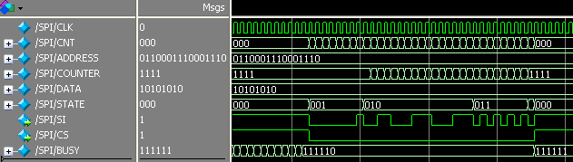
I’ve left out the declarations and initialises out so we can see what’s happening but basically we have 4 states that we cycle through, the write instruction, 16 bit address and the byte to write. We have an 8 bit counter CNT which is reset in each state so that we can count the cycle times of the clock, read the element from the array and write it to the SRAM.
It did take a while to get looking right, it’s a rough start but I found that it sometimes didn’t work correctly. This could be because I didn’t follow the SRAM datasheet as it requires a minimum of 1/2 clock cycle when at 3V for things such as CS setup and CS hold time.
if (UPDATECLK == 3) CLKout = ~CLKout;
if (UPDATECLK == 0 && CLKDELAY == 0) UPDATECLK = UPDATECLK + 2'd2;
UPDATECLK = UPDATECLK + 1'b1;
if (UPDATECLK == 3 && CLKout == 0) begin
...
I added in a clock divider (divide by 8) to slow down the communication as you can see above, we start the clock out once we put CS low (I had it running all the time before) and added in a read function too which turns on an LED if the write matches the read and it seems to work well, Download cpld_sram_read_write.
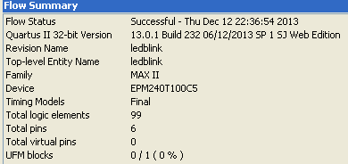
I added in an address variable later on so I could keep a counter of the address we are up to and then we can read up to a certain address and then stop however when you take the simulation and convert it to be synthesised but found that this variable took up at least 30 LEs itself even though it was only 16 bit which pushed the LEs used up to 99 LEs so it won’t fit the 64LE CPLD I was looking to put all this on eventually. To reduce the LEs used, I think a solution could be to pulse a pin when a write is complete and then the MCU can count/calculate which address the CPLD is up to.
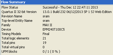
After removing most functionality from the CPLD, we should be able to use an ATtiny with V-USB to communicate with the PC, have the AVR configure the SRAM for sequential writing, begin the write and after writing the address to write to, we hand over to the CPLD to write the data and then stop after a while. We’re now down to 21 LEs even when we have 4 inputs and 4 outputs (the outputs could be separate SRAM chips).
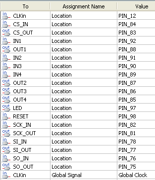
module sram (CLKin, RESET, LED,
IN1, IN2, IN3, IN4, OUT1, OUT2, OUT3, OUT4,
SI_IN, SI_OUT, SO_IN, SO_OUT, CS_IN, CS_OUT, SCK_IN, SCK_OUT);
...
always @ (posedge CLKin) begin
  if (!RESET) begin
    CYCLECOUNT <= 4'd7;
    LED <= 1'b0;
    UPDATECLK <= 2'd2;
    SI_OUT <= SI_IN;
    SO_OUT <= SO_IN;
    CS_OUT <= CS_IN;
    SCK_OUT <= SCK_IN;
  end
  else begin
  // Divide the main clock by 4
  if (UPDATECLK == 1) begin
    SCK_OUT <= ~SCK_OUT;
    UPDATECLK <= 2;
   end
  else UPDATECLK <= UPDATECLK + 1'b1;

    // If we are in a clock low, then do everything here
    if (UPDATECLK == 3 && SCK_OUT == 0) begin
      // Data
      OUT1 <= IN1;
      OUT2 <= IN2;
      OUT3 <= IN3;
      OUT4 <= IN4;
      SI_OUT <= IN1;

      if (CYCLECOUNT == 7) LED <= 1'b0;
      if (CYCLECOUNT == 0) begin
        CYCLECOUNT <= 7;
        LED <= 1'b1;
      end
    else CYCLECOUNT <= CYCLECOUNT - 1'b1;
    end
  end
end
endmodule
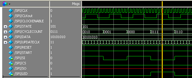
Here’s how it looks now, we now have a reset condition which resets all variables instead of using initialise which I’ve heard is something you shouldn’t use (except for simulation). Because the AVR needs to interface with the SRAM as well as the CPLD, when in the reset state, the CPLD basically re-directs the AVR’s SPI output/input to the SRAM. When it’s out of reset, the main clock is divided by 4, we count the clock cycles to 8 and in the clock low periods we sample the 4 inputs (but for the moment, I’m only sampling 1) and this continues until we are put back into reset. Download cpld_sram_write_data_modelsim and cpld_sram_write_data_quartus.
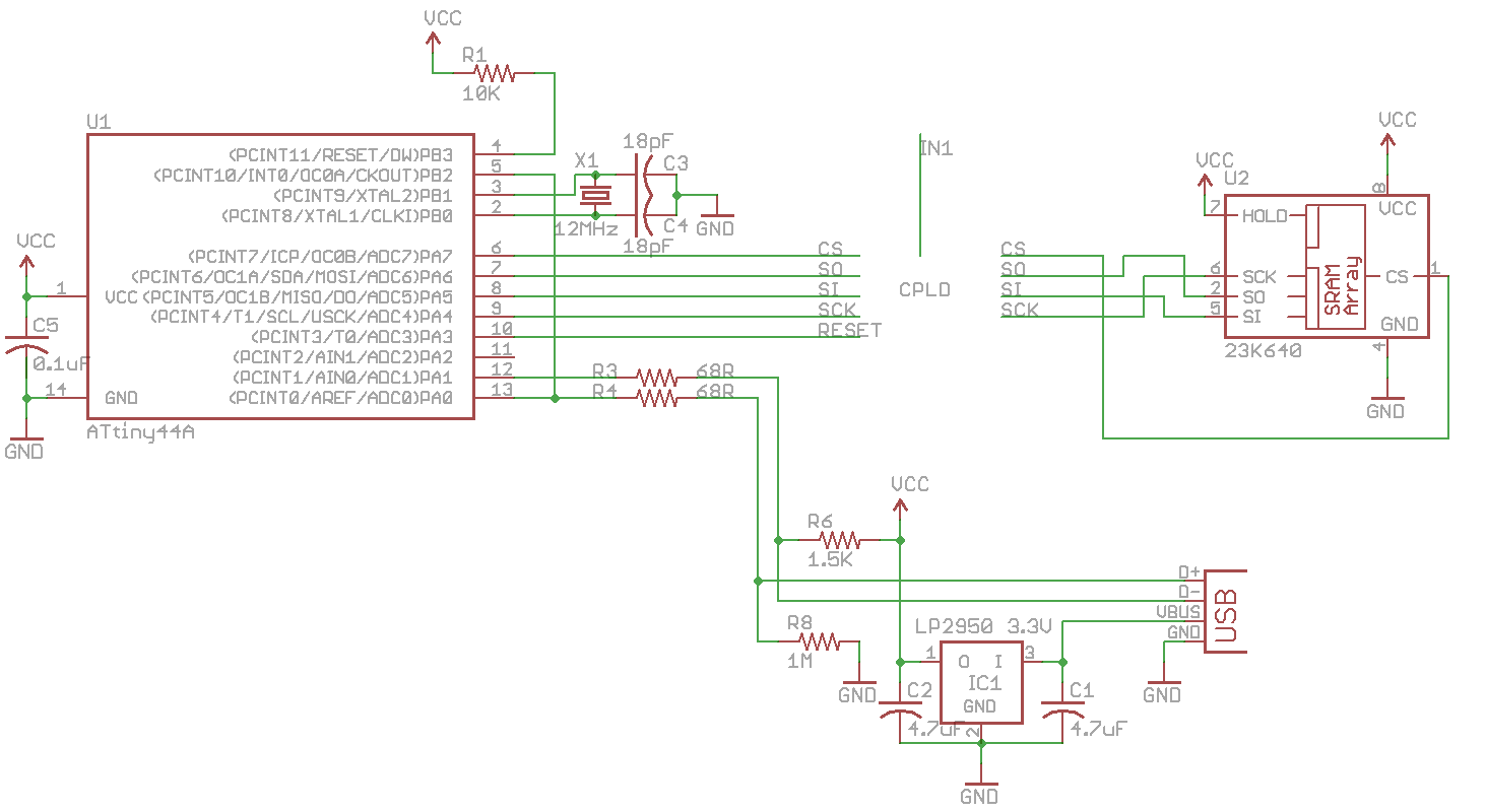
On the AVR, I’m using most of the code that I used on the SACL, just for testing this all out I only read up to the 1000 address, Download CPLD_Logic_Analyser_v0.1
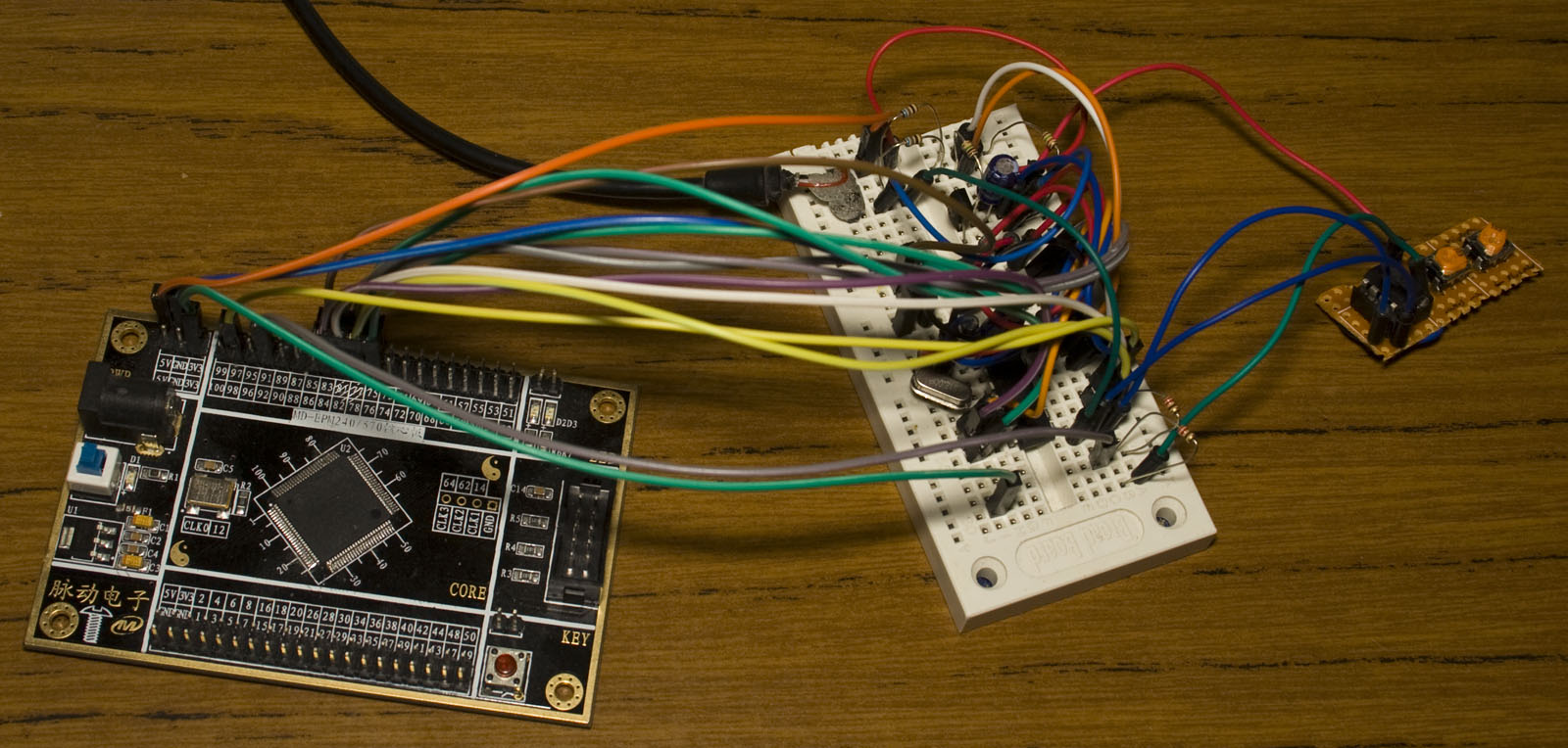
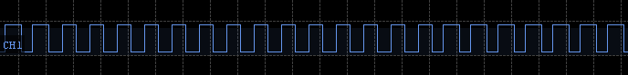
It seems to work hit and miss a bit, but I sense that’s because of the breadboard wiring. You can see that I’m using my ATtiny VCO to generate some waveforms to test out, here are the results of a 2KHz and 200KHz wave: 2khz wave /200khz wave
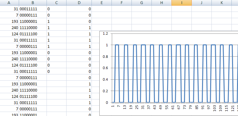
We can visualise the 200KHz wave in Excel as shown above but it doesn’t look that good: 200KHz
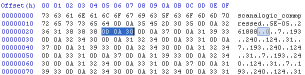
Since I have the Scanalogic analyser software I took a look at the format of the file and the old program’s .scl file seems easy enough to modify, the start of each byte of data is 0D 0A and then the number in this case 0. Each digit of the number is placed on it’s own byte such as 193 is split to 1, 9, 3. The 193 as you can see above in the excel shows that the signal went high (11) to low (00000) and then high again (1).
I made a little program to convert our decimal number input to the scl format, then pasted the output into the scl file manually and we can now see the waveform above which looks better: dec_to_scl. The only problem is now that the timing information on the Scanalogic software doesn’t match what our sampling rate really was.
For the next part I’ll need to increase the speed of the CPLD clock to 100MHz and see if I can find different SRAM options.
Building a CPLD Based Logic Analyser – Part 1: SPI writing in Verilog, Testing the basics and modifying Scanalogic SCL files to insert our own data
Building a CPLD Based Logic Analyser – Part 2: Switching to the EPM3064 CPLD
Building a CPLD Based Logic Analyser – Part 3: Testing the Cypress 1Mbit SRAM
Building a CPLD Based Logic Analyser – Part 4: Reading data/triggering with an ATmega with V-USB and testing
Building a CPLD Based Logic Analyser – Part 5: Prototype boards and fixing reading issues
Building a CPLD Based Logic Analyser – Part 6: Software side, trigger/sampling options, hardware changes and possible changes for a 100MHz analyser
Building a CPLD Based Logic Analyser – Part 7: PCBs arrived, move to Sigrok Pulseview, simple GUI program and a few software modifications


Maybe you can use open source software http://www.sump.org/projects/analyzer/client for visualization.