From our previous post, we made our prototyped PCBs which all worked together well. This time we just have a quick update – we’re making a few changes along with building acrylic cases/mounts for some of our boards.
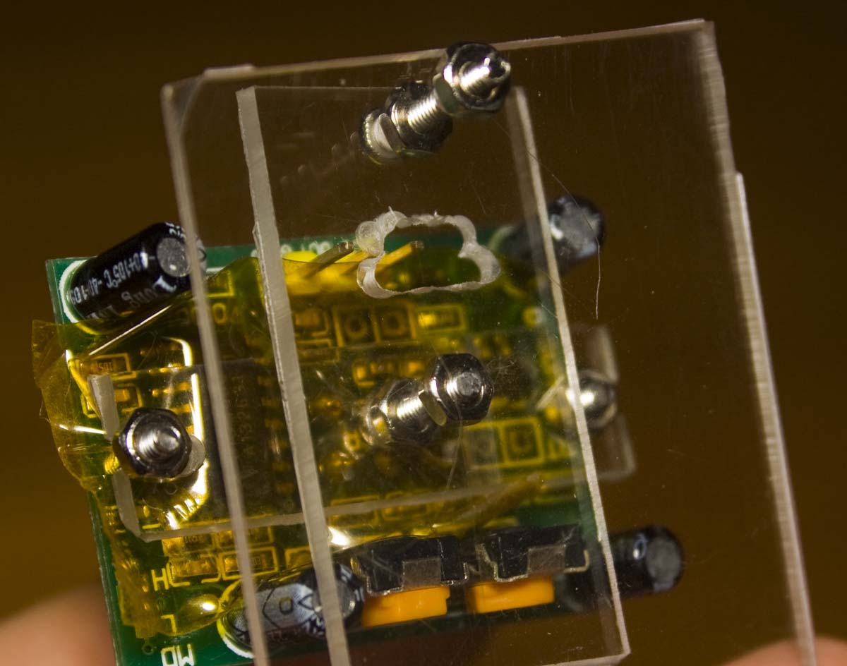
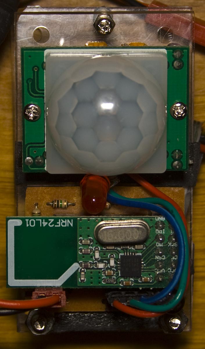
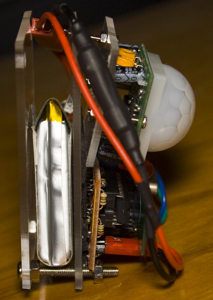
I’ve been rethinking my idea about using the existing plastic casing for the PIR, since I intended this to be a standalone alarm system I should really make my own case. We’ll need a way to mount the PIR sensor at an angle to the wall to point a bit downwards otherwise it’ll just point straight on and may not cover the whole room. Initially I started with the design above, there’s quite a bit of acrylic boards all screwed together with M2 screws.
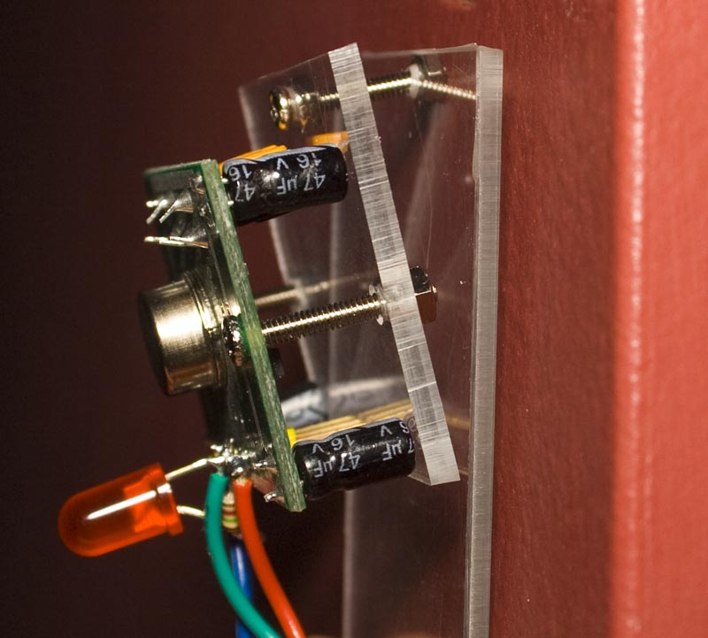
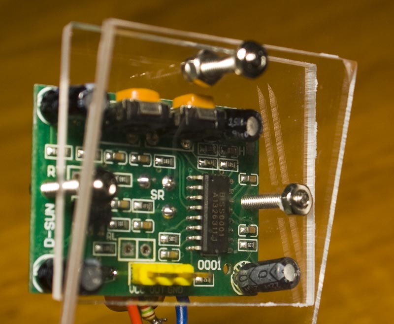
I went for a re-design and now it’s looking better with less parts being used. I’ll need to add some mounts to the ATtiny84 PIR PCB, switch the M3 screws that hold the Lipo in place with longer M2 screws and then add a small hole at the top so I can nail the bottom board to the wall and that will sort out the PIRs.
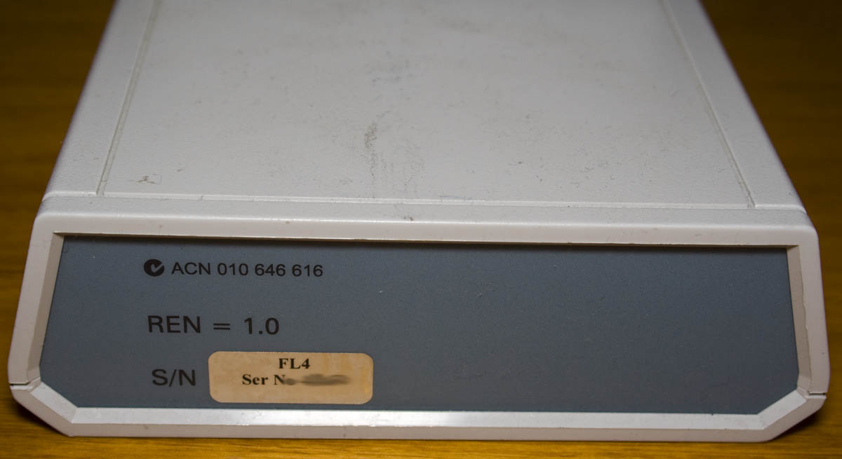
Today we’ll be taking a look at the Softlog Systems Faxlog 4 device which as it says converts incoming faxes to serial and then there’s another box which plugs into the PC. The date code is 2006/34th week.
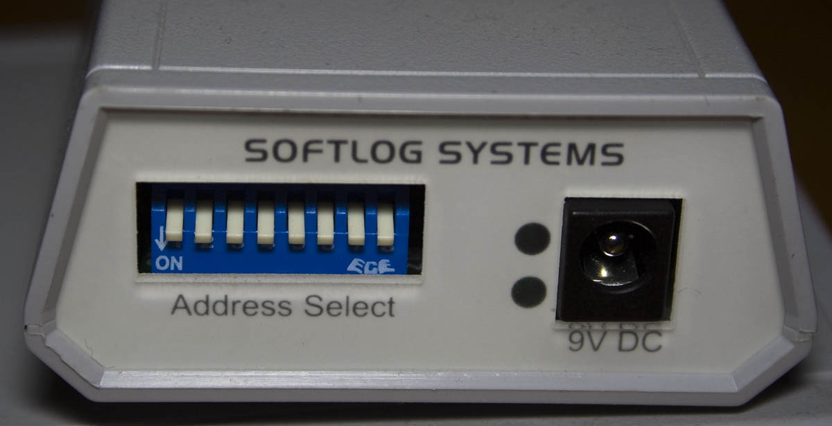
There was a RJ45 cable connecting this sub-board to the main board, whether or not this was all the parts in the Faxlog system is unknown. There is also a selectable address line via DIP switches.
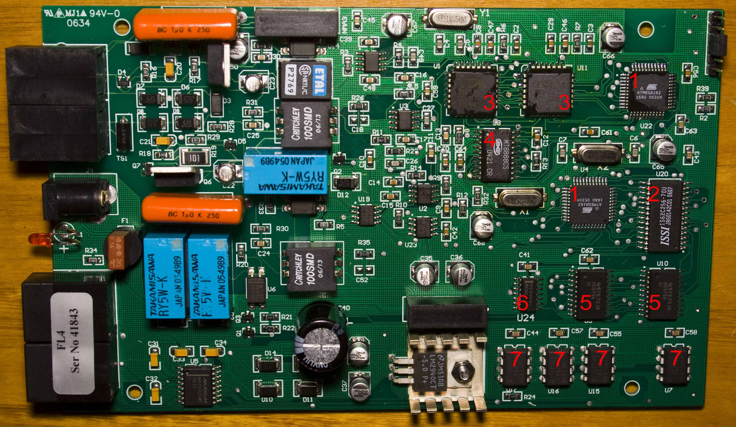
Main Board
The PCB has a lot more ICs and components than I had expected. We’ve got some phone line filtering and protection with some larger than normal capacitors (compared to internet routers), along with 2 TIP31CG NPN transistors, some RY5W-K relays, a NMV0515SC DC-DC converter 5V input to 15V output and some P2769 / 100SMD transformers. Coming from the transformers / opto-isolators, we’ve got 3 UA741 opamps and 2 DG419 analog switches. In terms of power supply side, it’s 9V input with a large 1000uF capacitor, LM2940CT 5V LDO with heatsink and a NMA0505DC 5V input to -5 and +5V output.
Ever since I did a teardown of the Squeezebox I wanted to re-use the Vacuum fluorescent display which is a MN32032A. It’s running off a 55V power supply, I was able to identify the data lines and by using my 8 channel logic analyser I took a few samples of the data.
Here’s the end result, it works to some degree, as you can see there is some signs of random pixels lighting up which I’ll need to look into at a later stage.
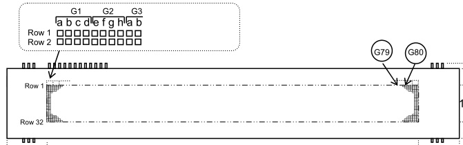
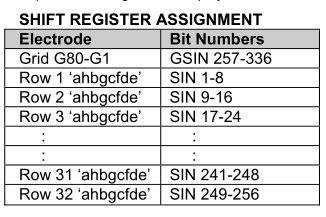
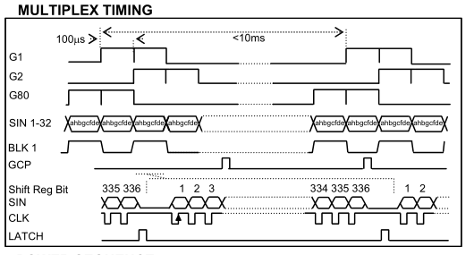
The VFD seems easy enough to use, it’s serial based where you shift out 336 bits containing 32 rows (32 bytes) and 80 grids (10 bytes) but we have to note that when we shift out each row byte it isn’t in the order of abcdefgh but rather ahbhcdfe and that each grid has controls only 4 lights per row. For example, if you were to turn on row 1 and turned on all the grids, a straight line would appear across the screen.
What we’re required to do is shift out 336 bits of which we need to turn on 2 grids at a time, latch the data and cycle GCP. If you do encounter ghosting you can turn the blanking (BLK) high for one time period and then low (however doing this didn’t help the problem I had). I’m not sure as to what the GCP line does but without it the display doesn’t work, it could mean grid control pulse?
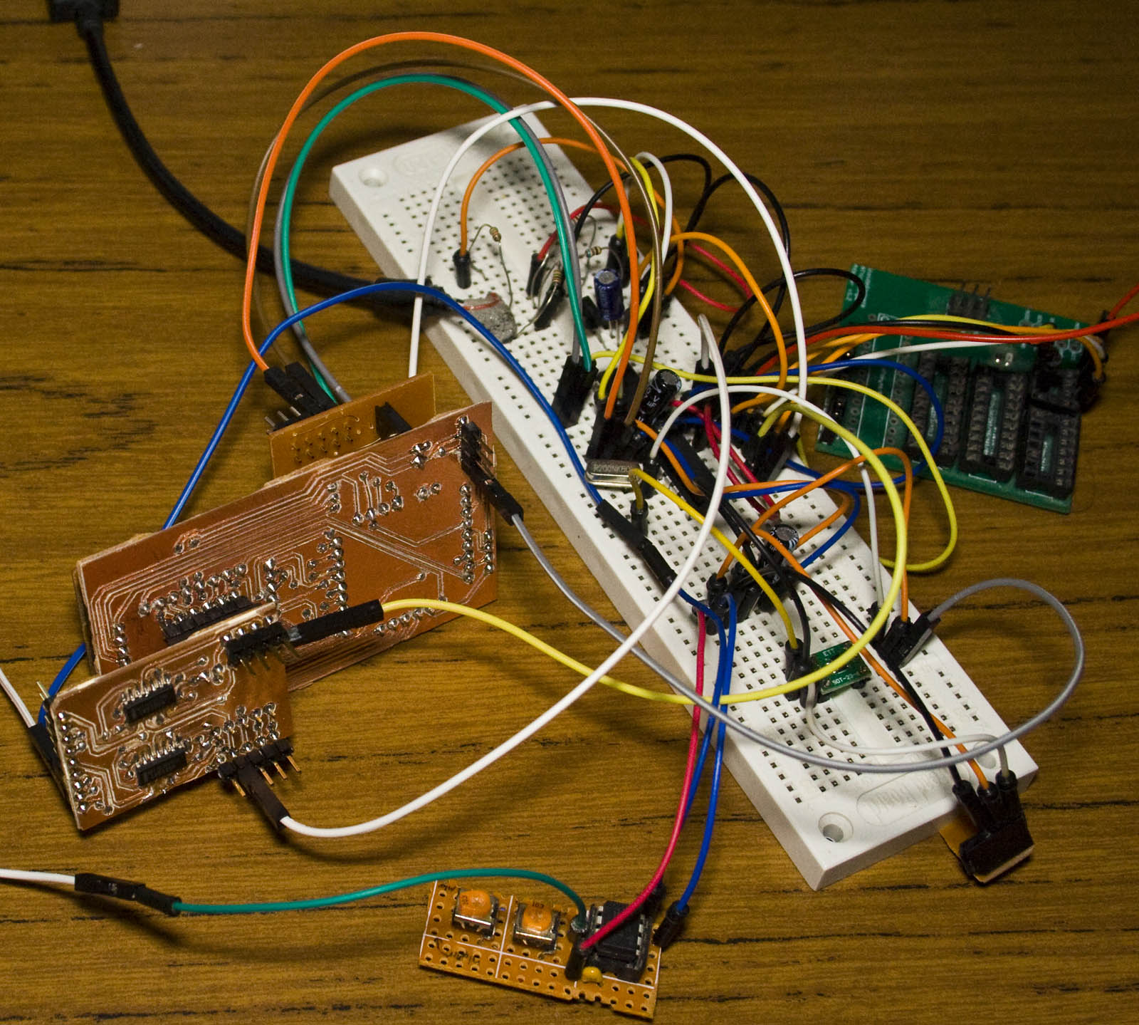
From our last part we made some prototype boards including the buffer board and fixed the reading issues. In this part we’ll look at the software side to display the data we extract, add trigger options/sample rates, some hardware changes and possible design changes which could give us an 100MHz logic analyser.
Software for displaying our data
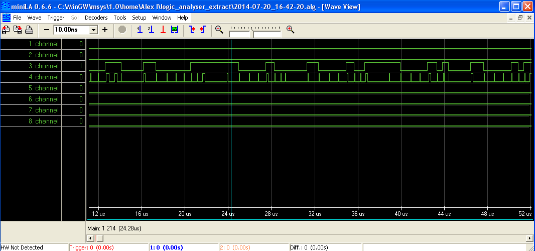
I had a look around at some software options that would just work out of the box and settled with one called MiniLA, they also had made an 100MHz logic analyser – it’s a beefier version of what I’m trying to achieve, their one has 32 channels and the CPLD/SRAM alone would cost $25-35 (about $40-50 in Australia) where as I’d like to make a small 8 channel one with USB (and it’s a learning experience for me too).
After looking around at the file format, it’s similar to how I was sending my data, so I was able to figure out how the data was formed – 00 00 FF 00 would set channel 1 to 8 all high for one time period. From the picture above, to change the time scale units from us to ns, you can change 41 to 42 and to change the time scale total length from say 2.52 to 2.62 ms you’d change 87 to 88. This should give us the flexibility to change time scale units depending on the clock we select.
Trigger/sample options
As the ATmega will act as the trigger source, I’ve been able to add options such as choosing which pin to trigger on, trigger level – high or low, trigger delay, trigger count – how many triggers we should wait for, sample rate and number of samples.
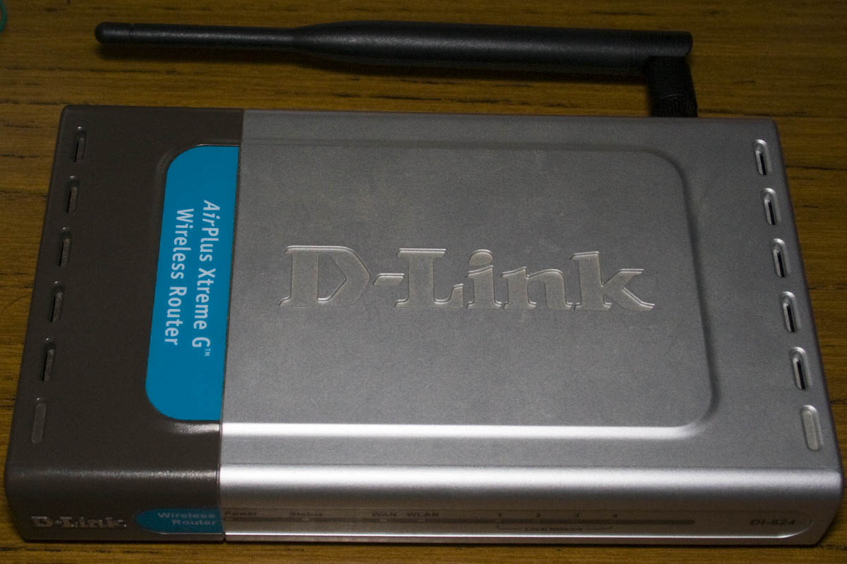
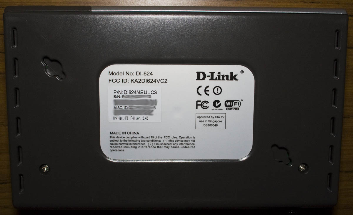
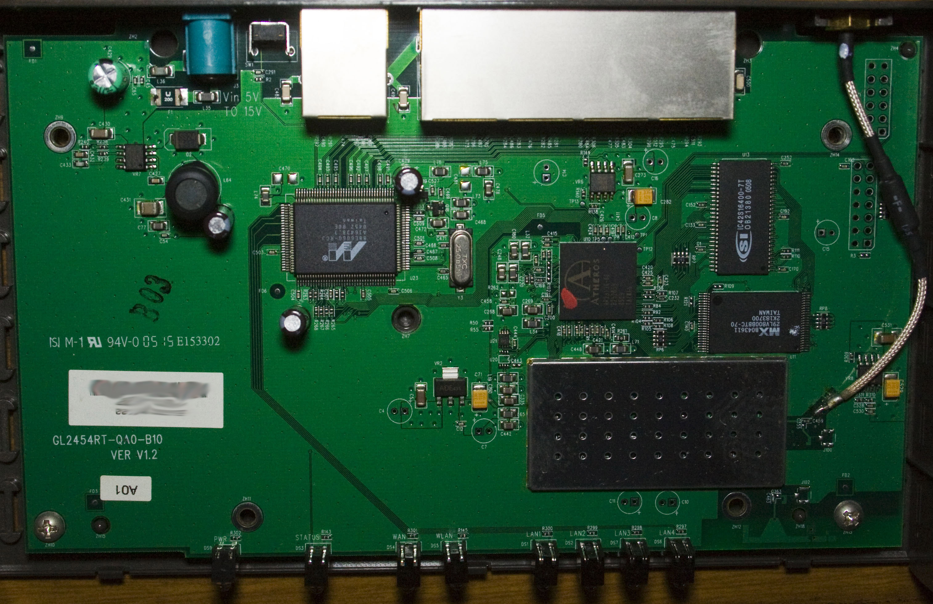
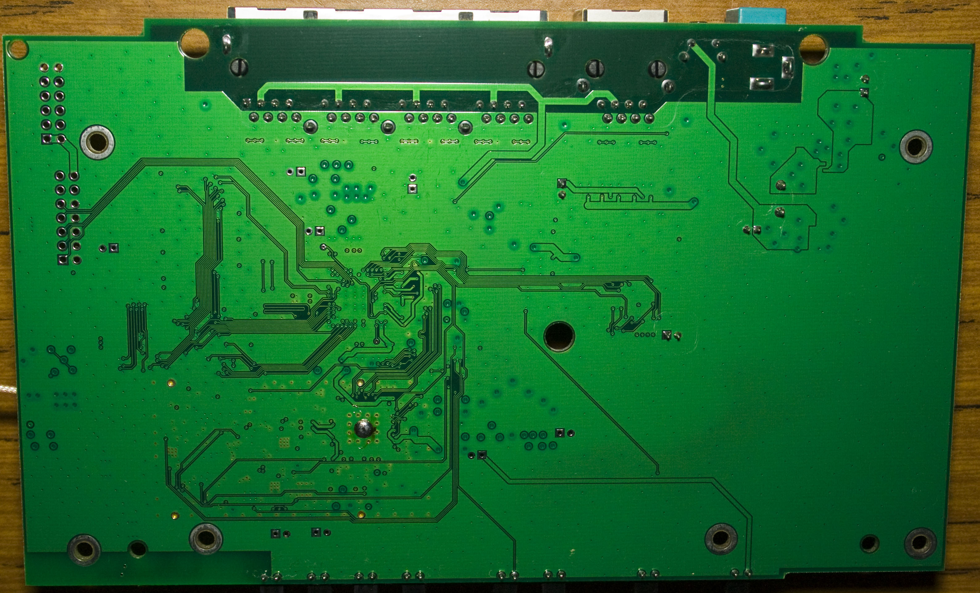
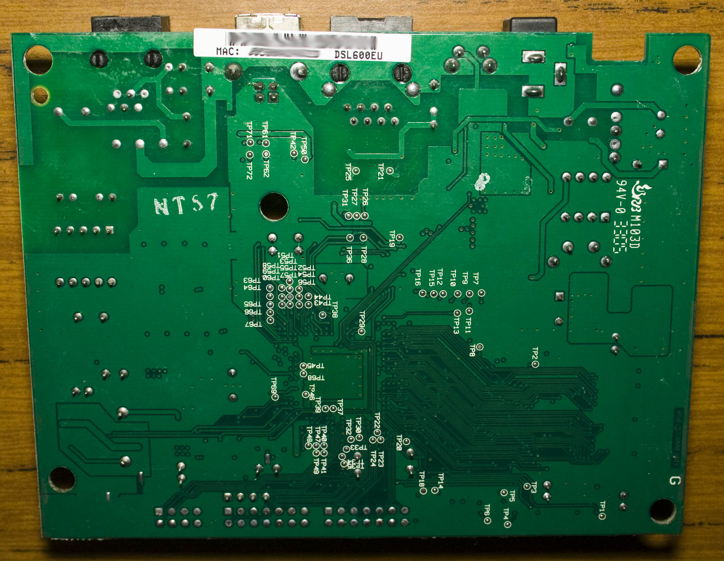
Today we’ll be taking a look at the D-Link AirPlus Xtreme G Wireless Router – a 4 port 10/100 ethernet and wireless router with 1 external antenna which has a date code of 2005/15th week.
Two screws later and we’re in.
At first glance the PCB is quite big and there’s a bit of empty space on it, they could have made it smaller if they really wanted to. We’ve got 4 chips plus a Wifi chip underneath the metal shield, an MPS MP1410ES SMPS on the input which can accept 5V to 15V, an ADE435 voltage regular near the metal shield and we have two AME AME8807 LDOs. Also we’ve got some tantalum capacitors which haven’t been too common in the routers I’ve seen.
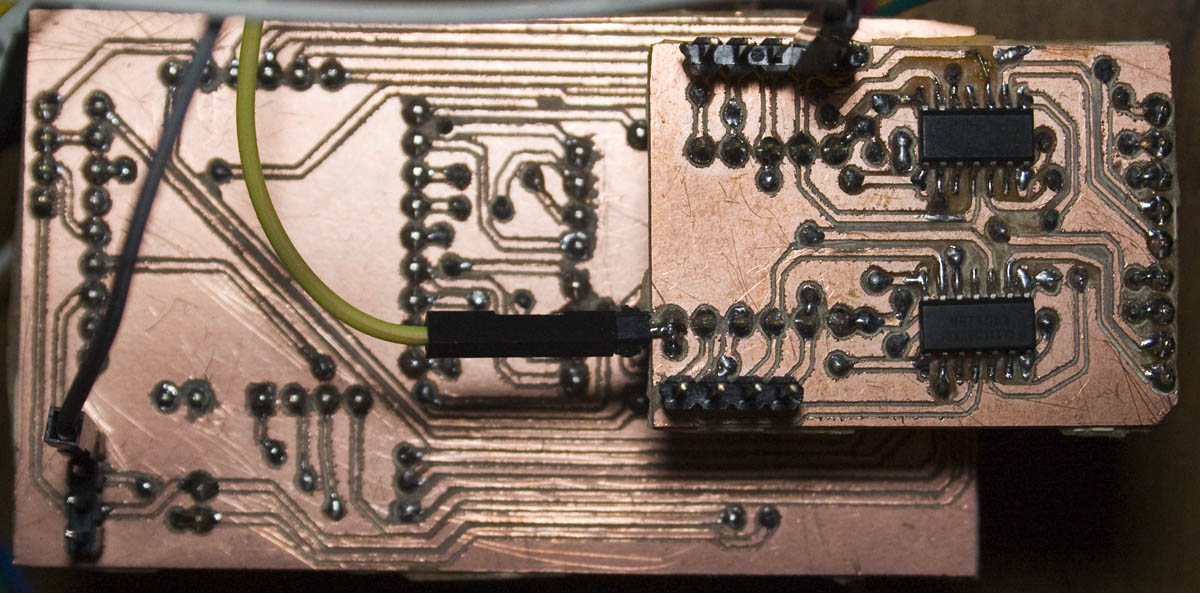
From our last part we were able to read the data from the SRAM using an ATmega but found that we couldn’t run the SRAM with a 100MHz clock and when reading the data out it was noisy/inaccurate – even re-reading the same address ranges would give different results. In this part, I’ve made some prototype boards and we’ll look into fixing the reading issues.
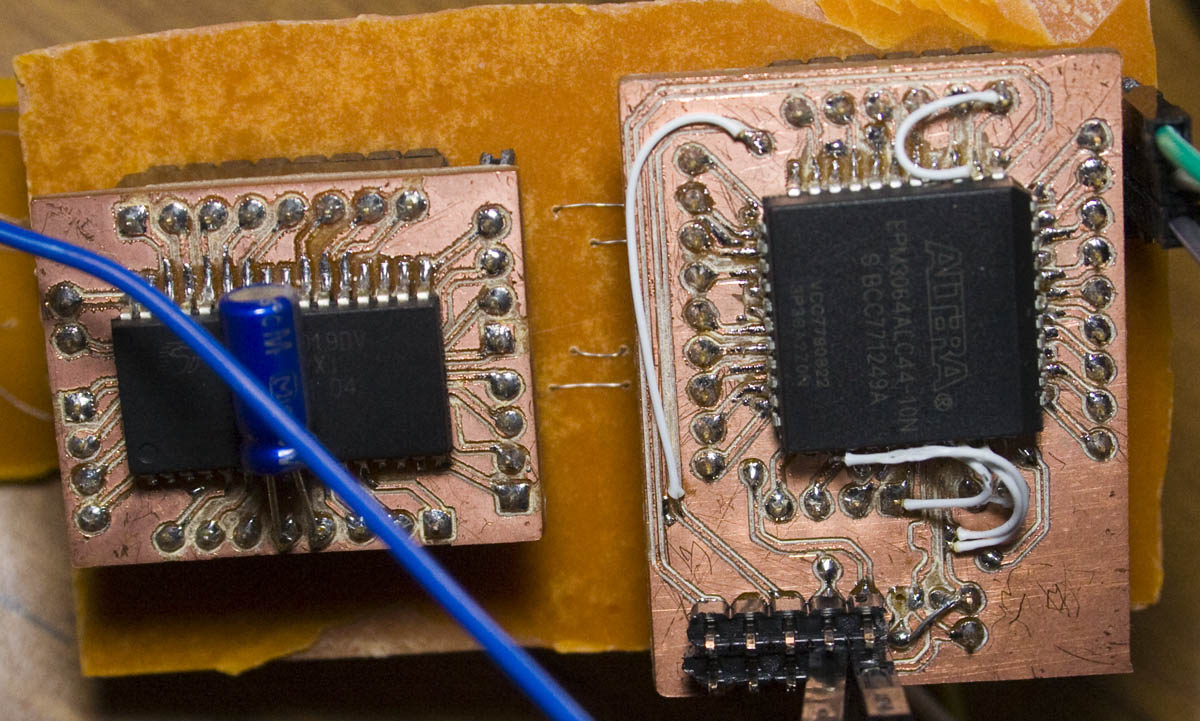
I decided to make a new board for the CPLD so I could mount it and the SRAM to a main board and also made a buffer logic board to be mounted under the main board plus there is also a very small board for the 50MHz oscillator.
For the buffer board, I’m using 2x 74LVC125 each one does 4 inputs. What I didn’t realise is that these are active low so I’ve modified my CPLD code to suit: CPLD_LogicAnalyser_v0.2
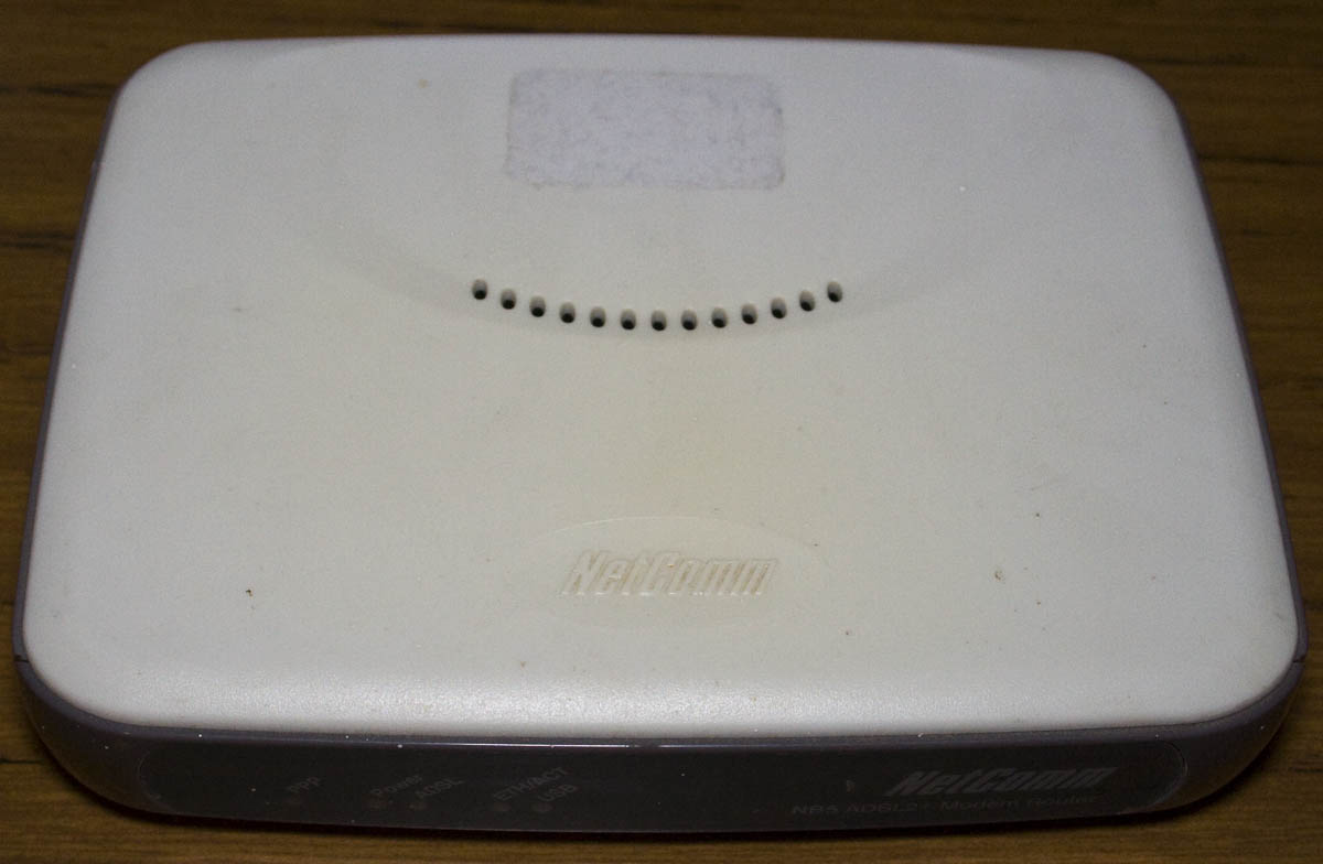
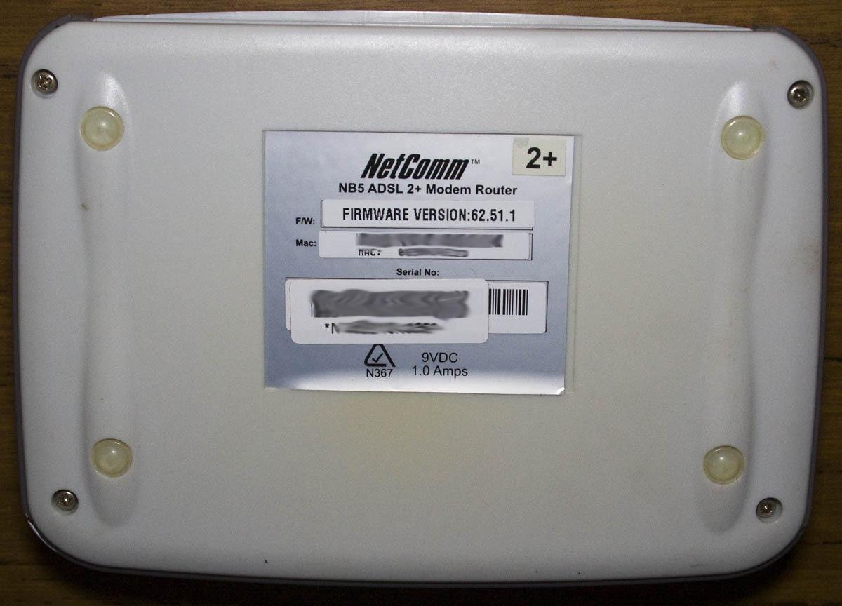
Today we’ll be taking a quick look at the Netcomm NB5 ADSL2+ Modem Router which has a date code of 2005/33rd week and a Ethernet/USB based modem/router. We’ve done a teardown of the NB5 ADSL version of this router before so lets how similar they are.
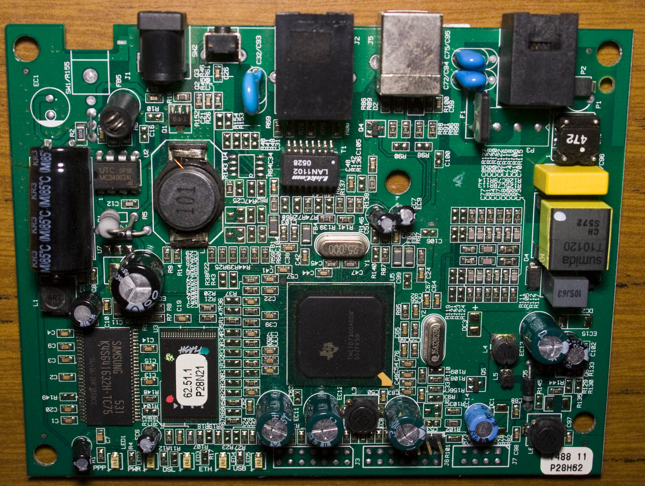
Some screws later and we’re in.
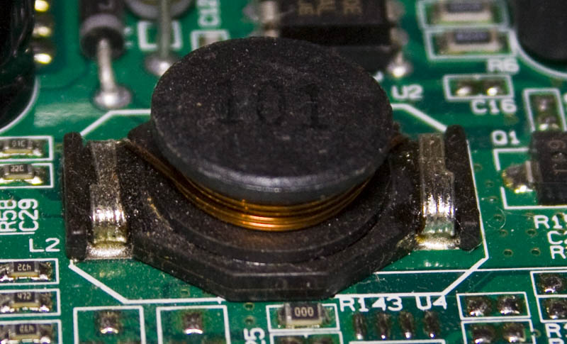
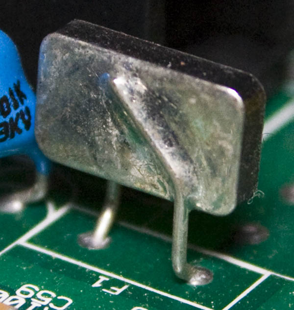
There are a few noticeable parts on the board, firstly the 3300uF 16V capacitor glued to the board (which has come off), a larger than usual 100uH inductor, a fuse with a metallic outer shell and they are using an MC34063 SMPS.
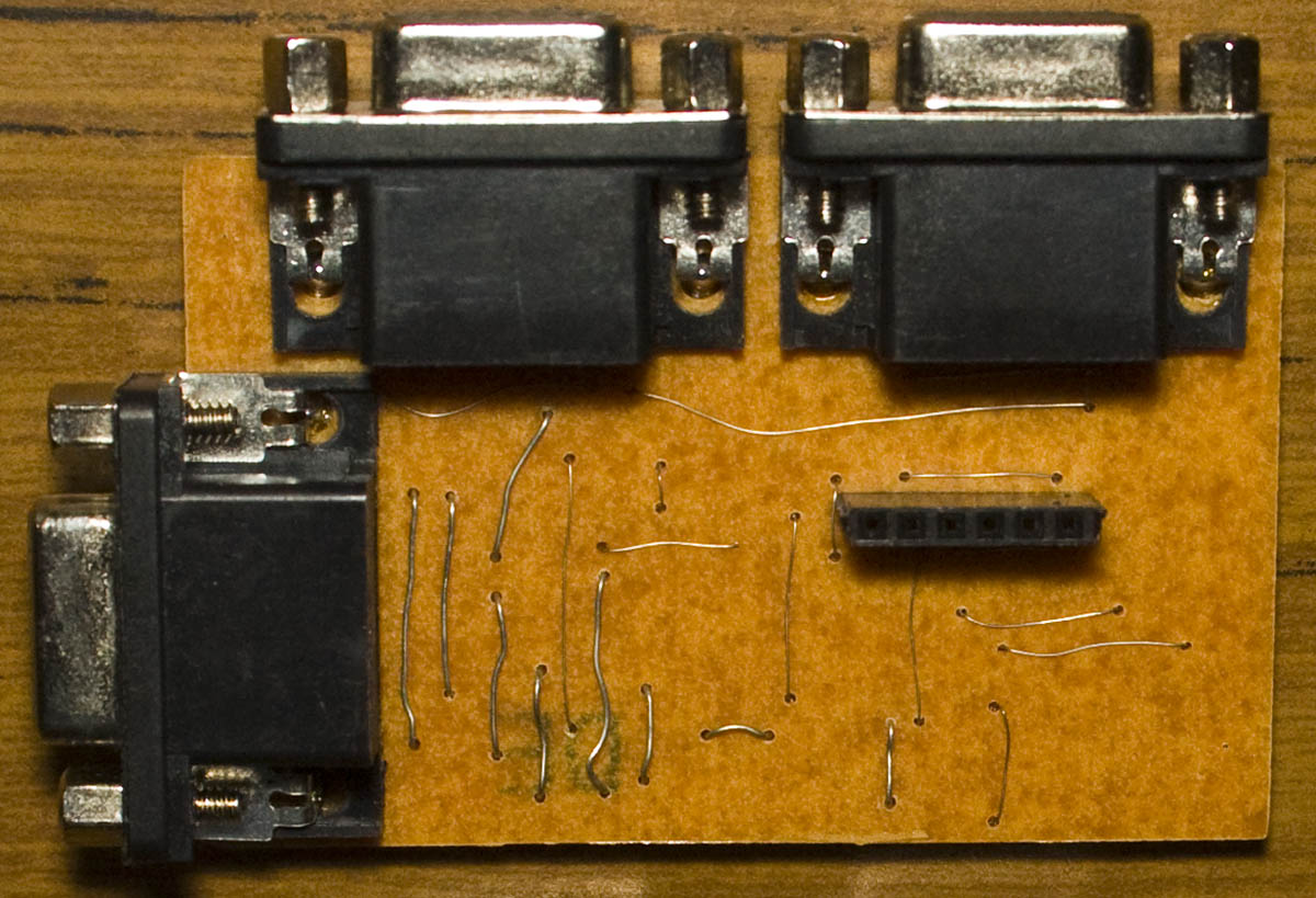
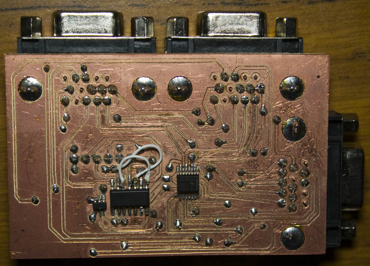
From our last part we chose the switches to use, the cabling idea to use network cables to connect to USB cables, the 7402 NOR gate to switch between inputs and gave it a test run on the VGA which worked. In this part we’ll put it all together and think about how we can add more input ports to do a 4, 8, 16 port KVM.
(sneak peak of KVM)
The first thing I did was test the 7402 NOR gate to see if there is an oscillation at startup, after a few attempts I found no issues but that you should tie unused gates to ground; even if it started in an unknown state, the state doesn’t change so it’s not too much of a concern for me.
I decided to have the VGA and USB boards separate as it would be easier to route them. The VGA board was built, there was a small mistake with choosing the wrong 7402 part in Eagle so I had to make a few modifications and it tested ok, there is a 6 pin header near the center to connect to the USB board.
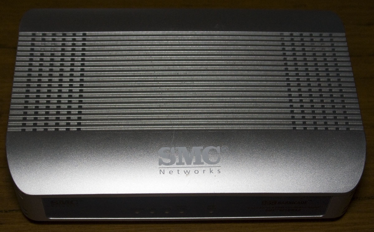
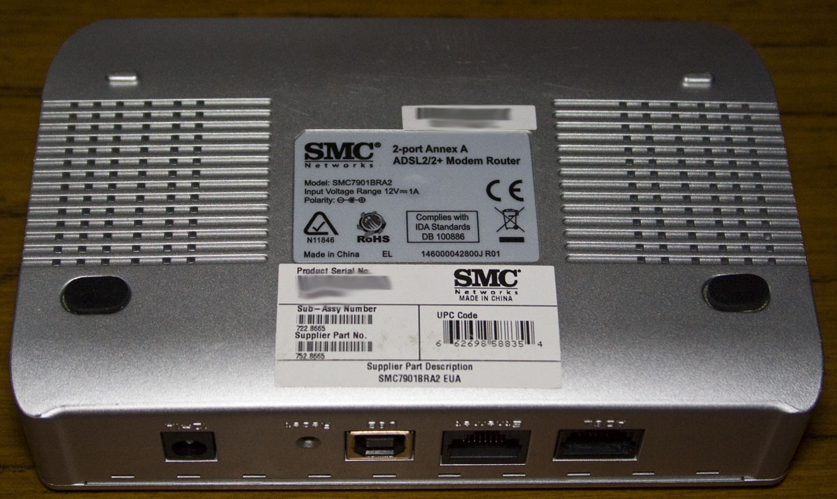
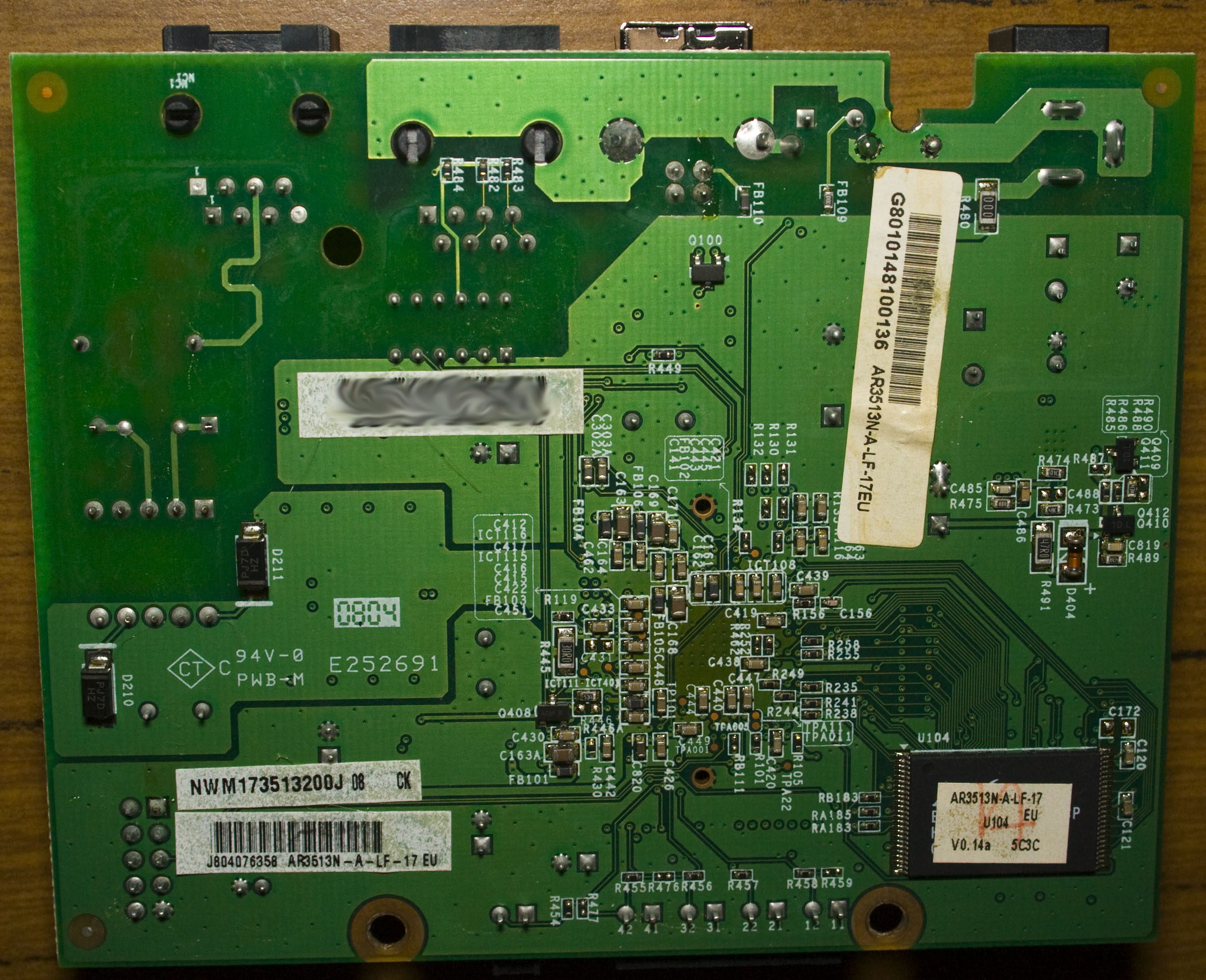
Today we’ll be taking a quick look at the SMC 2-Port Annex A ADSL2/2+ Modem Router (SMC7901BRA2) which has a date code of 2008/4th week and it’s a simple Ethernet or USB based modem/router.
Two screws later and we’re in.
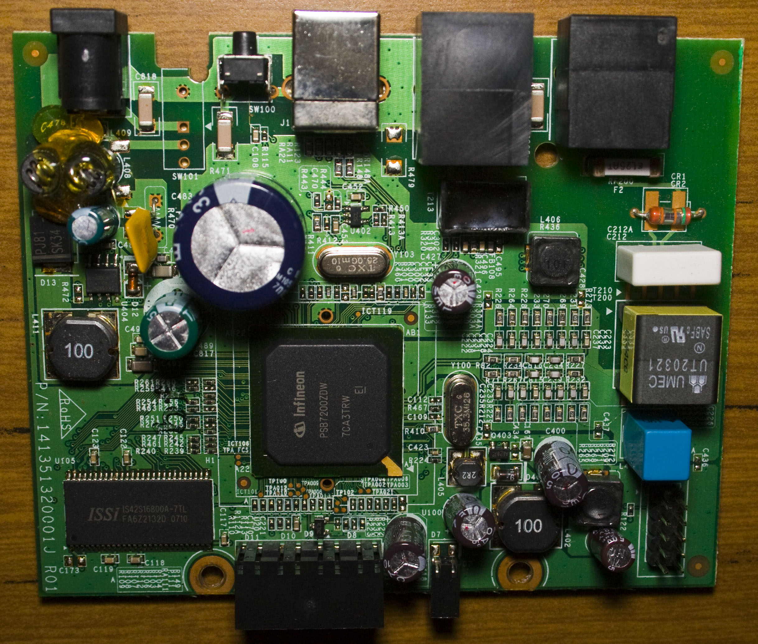
The first thing noticeable is the large Elcon 3300uF 25V capacitor near the middle of the board. There is a 6×2 pin header which is most likely a Jtag header, 2 crystals 35.3MHz and 25MHz and we have a Semitech SC4519H SMPS.
The main chip is an Infineon PSB7200ZDW XWAY AR7 with an ISSI IS42S16800A 128Mb SDRAM and an Eon EN29LV160AB-70TCP 16Mb Flash.
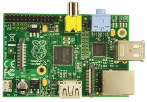
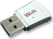
Ever since I built a Raspberry Pi 4-bay NAS in an existing Netgear NAS case I’ve been wanting to make a smaller custom acrylic version with just a 2.5” 750GB hard drive for either backups (like a small Synology) or a fileserver overall it should end up being quite small.
The main components of this project will be the Rapsberry Pi and Wi-pi adapter which I bought it from Element14 / Newark. Using the the Wi-Pi adapter I could make it all wireless.
Like my last NAS, I’ll be adding in a 16×2 LCD display to show the status, as I’ll be using a 2.5” drive all I’d need is a 5V 2-3A power adapter and a USB to SATA adapter of which I’ve found a better adapter that should be easier to plug the drive easier.
AdvanceVGA – Play your GBA on the big screen! Swap out the LCD for our board, solder some wires, connect 5V USB and VGA and you’re ready to go.
GBxCart RW allows you to backup GB/GBC/GBA ROMs, save or restore game saves and re-write supported flash carts. Mini RW option available for GB/GBC only.
Wireless Gameboy Controller – Use your Gameboy, mGB, GBC, GBA, GBA SP, GB Micro, NDS and NDS Lite as a wireless controller on Windows, Linux, Raspberry Pi, etc, and on your NES, SNES, N64, Gamecube and Wii.